Advanced Semiconductor Photomask Market Overview
Semiconductor Photomasks are high-purity quartz or glass plates that contain a pattern of ICs. These are used in the reproduction of pattern structures for manufacturing printed circuit boards, electronic circuits, and LCD displays, and for the serial production of reticles and other microstructures. Semiconductor Photomasks are used at wavelengths of 365 nm, 248 nm, and 193 nm. ICs are manufactured layer by layer, where each layer requires a unique Semiconductor Photomask. As current generation ICs typically have 25-60 layers, the manufacturing process of Semiconductor Photomasks has become complex.
This report provides a deep insight into the global Advanced Semiconductor Photomask market covering all its essential aspects. This ranges from a macro overview of the market to micro details of the market size, competitive landscape, development trend, niche market, key market drivers and challenges, SWOT analysis, value chain analysis, etc.
The analysis helps the reader to shape the competition within the industries and strategies for the competitive environment to enhance the potential profit. Furthermore, it provides a simple framework for evaluating and accessing the position of the business organization. The report structure also focuses on the competitive landscape of the Global Advanced Semiconductor Photomask Market, this report introduces in detail the market share, market performance, product situation, operation situation, etc. of the main players, which helps the readers in the industry to identify the main competitors and deeply understand the competition pattern of the market.
In a word, this report is a must-read for industry players, investors, researchers, consultants, business strategists, and all those who have any kind of stake or are planning to foray into the Advanced Semiconductor Photomask market in any manner.
Advanced Semiconductor Photomask Market Analysis:
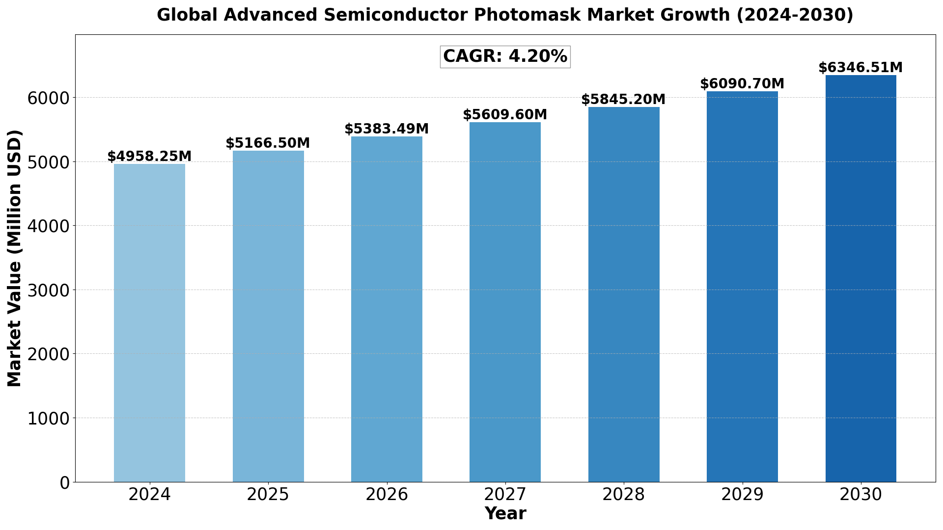
The Global Advanced Semiconductor Photomask Market size was estimated at USD 4758.40 million in 2023 and is projected to reach USD 6346.51 million by 2030, exhibiting a CAGR of 4.20% during the forecast period.
North America Advanced Semiconductor Photomask market size was USD 1239.90 million in 2023, at a CAGR of 3.60% during the forecast period of 2024 through 2030.
Access Your Free Sample Report Now
Advanced Semiconductor Photomask Key Market Trends :
1. Rising Demand for EUV Photomasks
- The adoption of extreme ultraviolet (EUV) lithography for advanced nodes (e.g., 7nm, 5nm, 3nm, and below) is driving demand for EUV photomasks.
- These photomasks require specialized materials and manufacturing techniques, leading to significant investments in EUV mask production capabilities.
2. Shift Towards Multi-Patterning Lithography
- For nodes where EUV is not yet widely adopted, multi-patterning techniques such as double patterning and quadruple patterning are being used.
- This increases the number of photomasks required per wafer, driving market growth.
3. Advancements in Mask Materials and Durability
- Innovations in photomask materials, such as phase-shifting masks and attenuated phase-shifting masks, are improving the precision of light transmission and patterning.
- There is also a focus on enhancing the durability of masks to withstand repeated use in high-volume production.
4. Integration of AI and Machine Learning in Mask Design
- AI-driven photomask design is becoming more prevalent to optimize patterns, reduce defects, and improve manufacturing efficiency.
- Computational lithography and simulation tools are being utilized to create highly accurate masks for complex patterns.
5. Increased Investments in Photomask Inspection and Repair
- As chip designs become more intricate, the need for defect-free photomasks has intensified, leading to increased investments in inspection and repair technologies.
- Advanced techniques like electron beam inspection (e-beam) and actinic inspection are gaining traction for high-precision mask quality assurance.
Advanced Semiconductor Photomask Market Regional Analysis :
1. North America (USA, Canada, Mexico)
- USA: The largest market in the region due to advanced infrastructure, high disposable income, and technological advancements. Key industries include technology, healthcare, and manufacturing.
- Canada: Strong market potential driven by resource exports, a stable economy, and government initiatives supporting innovation.
- Mexico: A growing economy with strengths in automotive manufacturing, agriculture, and tourism, benefitting from trade agreements like the USMCA.
2. Europe (Germany, UK, France, Russia, Italy, Rest of Europe)
- Germany: The region’s industrial powerhouse with a focus on engineering, automotive, and machinery.
- UK: A hub for financial services, fintech, and pharmaceuticals, though Brexit has altered trade patterns.
- France: Strong in luxury goods, agriculture, and aerospace with significant innovation in renewable energy.
- Russia: Resource-driven economy with strengths in oil, gas, and minerals but geopolitical tensions affect growth.
- Italy: Known for fashion, design, and manufacturing, especially in luxury segments.
- Rest of Europe: Includes smaller yet significant economies like Spain, Netherlands, and Switzerland with strengths in finance, agriculture, and manufacturing.
3. Asia-Pacific (China, Japan, South Korea, India, Southeast Asia, Rest of Asia-Pacific)
- China: The largest market in the region with a focus on technology, manufacturing, and e-commerce. Rapid urbanization and middle-class growth fuel consumption.
- Japan: Technological innovation, particularly in robotics and electronics, drives the economy.
- South Korea: Known for technology, especially in semiconductors and consumer electronics.
- India: Rapidly growing economy with strengths in IT services, agriculture, and pharmaceuticals.
- Southeast Asia: Key markets like Indonesia, Thailand, and Vietnam show growth in manufacturing and tourism.
- Rest of Asia-Pacific: Emerging markets with growing investment in infrastructure and services.
4. South America (Brazil, Argentina, Colombia, Rest of South America)
- Brazil: Largest economy in the region, driven by agriculture, mining, and energy.
- Argentina: Known for agriculture exports and natural resources but faces economic instability.
- Colombia: Growing economy with strengths in oil, coffee, and flowers.
- Rest of South America: Includes Chile and Peru, which have strong mining sectors.
5. The Middle East and Africa (Saudi Arabia, UAE, Egypt, Nigeria, South Africa, Rest of MEA)
- Saudi Arabia: Oil-driven economy undergoing diversification with Vision 2030 initiatives.
- UAE: Financial hub with strengths in tourism, real estate, and trade.
- Egypt: Growing infrastructure development and tourism.
- Nigeria: Largest economy in Africa with strengths in oil and agriculture.
- South Africa: Industrialized economy with strengths in mining and finance.
- Rest of MEA: Includes smaller yet resource-rich markets like Qatar and Kenya with growing infrastructure investments.
Advanced Semiconductor Photomask Market Segmentation :
The research report includes specific segments by region (country), manufacturers, Type, and Application. Market segmentation creates subsets of a market based on product type, end-user or application, Geographic, and other factors. By understanding the market segments, the decision-maker can leverage this targeting in the product, sales, and marketing strategies. Market segments can power your product development cycles by informing how you create product offerings for different segments.
Market Segmentation (by Type)
- Quartz Mask
- Soda Mask
- Relief Plate
Market Segmentation (by Application)
- Semiconductor
- Flat Panel Display
- Touch Industry
- Circuit Board
Advanced Semiconductor Photomask Market Competitive landscape :
- Photronics
- Toppan
- DNP
- Hoya
- SK-Electronics
- LG Innotek
- ShenZheng QingVi
- Taiwan Mask
- Nippon Filcon
- Compugraphics
- Newway Photomask
Download Your Complimentary Sample Report
Drivers
- Advancements in Semiconductor Technology
As the semiconductor industry progresses toward smaller nodes (e.g., 7nm, 5nm, 3nm) and advanced chip designs like 3D stacking and FinFET, there is an increasing need for high-precision photomasks. These masks are essential in photolithography processes, enabling the production of intricate and highly miniaturized chip features. - Demand for High-Performance Electronics
The growth in consumer electronics, including smartphones, tablets, and wearables, is driving the need for advanced semiconductor manufacturing. These devices require chips that are smaller, faster, and more power-efficient, which directly increases the demand for sophisticated photomasks. - Proliferation of 5G and IoT Devices
The rollout of 5G technology and the widespread adoption of IoT devices require advanced semiconductors that need intricate photomasks for fabrication. These next-generation devices demand higher transistor densities, driving the need for finer patterns and more advanced photomask technologies. - Growth in Automotive Electronics and EVs
With the increasing demand for automotive electronics, particularly in electric vehicles (EVs) and advanced driver-assistance systems (ADAS), the need for more complex semiconductor chips is growing. This requires advanced photomasks capable of supporting the high-precision manufacturing of power management systems, sensors, and other critical components. - Increase in Semiconductor Fabrication Plants (Fabs)
The expansion of semiconductor manufacturing facilities globally, especially in regions like the U.S. and Asia-Pacific, is increasing demand for advanced photomasks. New fabs need state-of-the-art photomasks to meet the growing requirements for advanced node manufacturing.
Restraints
- High Cost of Advanced Photomasks
The development of advanced photomasks, especially for smaller nodes (e.g., 5nm and beyond), is a costly process. Photomasks for cutting-edge nodes require precision, high-quality materials, and extensive testing, making them expensive. These costs may limit adoption, particularly among smaller manufacturers or those with tight budgets. - Technological Complexity and Long Development Time
The design and production of photomasks for advanced nodes involve highly specialized technologies and can take significant time to develop and qualify. This complexity leads to longer development cycles and delays in the availability of the latest technologies. - Vulnerability to Contamination
Photomasks are highly susceptible to contamination during production and use. Even minute particles or defects can affect the photolithography process, leading to defects in semiconductor chips. Ensuring photomask cleanliness and quality control is a significant challenge in the manufacturing process. - Limited Availability of Expertise and Equipment
The production of photomasks for advanced semiconductor nodes requires specialized equipment and highly skilled labor. This creates a bottleneck in the supply chain, as only a few companies have the capability to manufacture photomasks for cutting-edge semiconductor technologies.
Opportunities
- Growth in Emerging Technologies (AI, ML, Quantum Computing)
The increasing demand for advanced semiconductor chips for emerging technologies like artificial intelligence (AI), machine learning (ML), and quantum computing presents a significant opportunity for advanced photomask manufacturers. These technologies require high-performance chips with complex designs that demand precision photomasks. - Development of Next-Generation Lithography Techniques
Emerging lithography techniques such as Extreme Ultraviolet (EUV) lithography and multi-patterning are providing new opportunities for photomask manufacturers. These technologies enable the production of even smaller and more intricate patterns on semiconductor wafers, driving the need for advanced photomasks that can support these new processes. - Demand for Photomasks in the Semiconductor Ecosystem Beyond Traditional Chips
Advanced photomasks are increasingly being used in applications outside traditional microprocessors, such as sensors, MEMS (Micro-Electro-Mechanical Systems), and optoelectronics. This broadens the market potential and provides growth opportunities in diverse sectors like automotive, healthcare, and renewable energy. - Regional Expansion of Semiconductor Production
The push for localized semiconductor manufacturing in regions like the U.S., Europe, and Southeast Asia is creating new demand for photomasks. As these regions invest in fabs and infrastructure, there will be an increasing need for advanced photomasks to support local production. - R&D Investments for Custom Photomasks
Semiconductor companies are increasingly investing in custom photomasks tailored to their specific requirements. This trend presents an opportunity for photomask manufacturers to offer specialized solutions for niche applications or for advanced semiconductor nodes.
Challenges
- Rapid Technological Evolution
The semiconductor industry is evolving rapidly, with new nodes and architectures emerging at a fast pace. Photomask manufacturers must continually innovate to keep up with these technological changes. The constant need for new mask designs can strain resources and increase development costs. - Challenges in Scaling for Smaller Nodes
As semiconductor nodes shrink, photomasks must be more precise and intricate. The shift to advanced nodes, such as 3nm and 2nm, presents challenges in scaling photomask technology to handle increasingly complex patterns without defects. - Cost and Complexity of EUV Lithography
The adoption of EUV lithography for advanced nodes requires extremely high-precision photomasks. EUV systems are expensive, and the photomasks used with EUV lithography must meet even more stringent quality standards, further increasing costs. - Intense Competition and Consolidation
The advanced photomask market is highly competitive, with a limited number of players capable of meeting the stringent requirements for cutting-edge semiconductor manufacturing. This intense competition, along with the high barriers to entry, can lead to market consolidation and may limit opportunities for new entrants.
Key Benefits of This Market Research:
- Industry drivers, restraints, and opportunities covered in the study
- Neutral perspective on the market performance
- Recent industry trends and developments
- Competitive landscape & strategies of key players
- Potential & niche segments and regions exhibiting promising growth covered
- Historical, current, and projected market size, in terms of value
- In-depth analysis of the Semiconductor Lens Market
- Overview of the regional outlook of the Semiconductor Lens Market:
Key Reasons to Buy this Report:
- Access to date statistics compiled by our researchers. These provide you with historical and forecast data, which is analyzed to tell you why your market is set to change
- This enables you to anticipate market changes to remain ahead of your competitors
- You will be able to copy data from the Excel spreadsheet straight into your marketing plans, business presentations, or other strategic documents
- The concise analysis, clear graph, and table format will enable you to pinpoint the information you require quickly
- Provision of market value (USD Billion) data for each segment and sub-segment
- Indicates the region and segment that is expected to witness the fastest growth as well as to dominate the market
- Analysis by geography highlighting the consumption of the product/service in the region as well as indicating the factors that are affecting the market within each region
- Competitive landscape which incorporates the market ranking of the major players, along with new service/product launches, partnerships, business expansions, and acquisitions in the past five years of companies profiled
- Extensive company profiles comprising of company overview, company insights, product benchmarking, and SWOT analysis for the major market players
- The current as well as the future market outlook of the industry concerning recent developments which involve growth opportunities and drivers as well as challenges and restraints of both emerging as well as developed regions
- Includes in-depth analysis of the market from various perspectives through Porters five forces analysis
- Provides insight into the market through Value Chain
- Market dynamics scenario, along with growth opportunities of the market in the years to come
- 6-month post-sales analyst support
In case of any queries or customization requirements, please connect with our sales team, who will ensure that your requirements are met.
FAQs
Get Sample Report PDF for Exclusive Insights
Report Sample Includes
- Table of Contents
- List of Tables & Figures
- Charts, Research Methodology, and more...