MARKET INSIGHTS
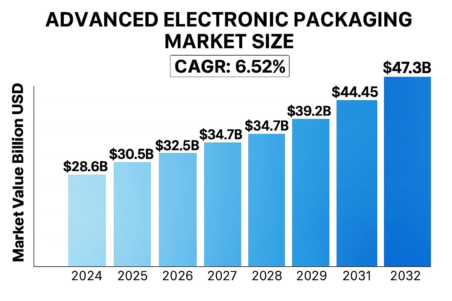
The global Advanced Electronic Packaging Market was valued at US$ 28.6 billion in 2024 and is projected to reach US$ 47.3 billion by 2032, at a CAGR of 6.52% during the forecast period 2025-2032.
Advanced electronic packaging involves the design and manufacturing of protective enclosures for electronic components ranging from individual semiconductor chips to complete systems. These solutions ensure performance reliability while addressing challenges like miniaturization, thermal management, and signal integrity. Key packaging types include metal packages for high-reliability applications, plastic packages for cost-sensitive mass production, and ceramic packages for superior thermal and electrical properties.
Market growth is driven by surging demand in semiconductor manufacturing, particularly for AI chips and 5G components, where packaging accounts for 30-40% of total production costs. While Asia-Pacific dominates production with 65% market share, North America leads in R&D investment with major players like DuPont and Ametek launching advanced materials. Recent developments include Panasonic’s 2023 introduction of high-density interconnect substrates for automotive electronics and Shinko Electric’s expansion of flip-chip packaging capacity to meet data center demand.
MARKET DYNAMICS
MARKET DRIVERS
Rising Demand for Miniaturized Electronics Accelerates Advanced Packaging Adoption
The global push toward smaller, more powerful electronic devices is driving unprecedented demand for advanced packaging solutions. With smartphone manufacturers incorporating increasingly sophisticated components and IoT devices shrinking in size while expanding functionality, the need for innovative packaging technologies has never been greater. High-density interconnect (HDI) technologies alone are projected to grow at a compound annual growth rate of nearly 11% over the next five years as they enable more components to fit into smaller spaces.
5G Infrastructure Deployment Creates New Packaging Requirements
The global rollout of 5G networks represents a significant catalyst for the advanced electronic packaging market. 5G base stations require high-frequency, heat-resistant packaging solutions that can operate reliably under demanding conditions. This has led to increased adoption of ceramic and advanced plastic packages that offer superior thermal management properties. The telecommunications sector’s investment in 5G infrastructure is expected to generate over 25% of total demand for advanced packaging materials by 2025.
Automotive Electronics Revolution Demands Robust Packaging Solutions
The automotive industry’s transition toward electric vehicles and autonomous driving systems is creating substantial opportunities for advanced packaging providers. Modern vehicles now incorporate hundreds of electronic control units, each requiring reliable packaging that can withstand vibration, extreme temperatures, and harsh environmental conditions. The automotive electronics market’s growth at approximately 8% annually reflects this increasing demand, with packaging solutions playing a critical role in ensuring component reliability.
MARKET RESTRAINTS
High Material Costs and Complex Manufacturing Processes Limit Market Expansion
While demand grows, the advanced packaging industry faces significant cost barriers. The specialized materials required for high-performance packages, particularly in the ceramic segment, often carry premium price points that can be 3-5 times higher than conventional packaging materials. These costs become particularly prohibitive for price-sensitive applications, limiting market penetration in consumer electronics and other cost-driven sectors.
Supply Chain Vulnerabilities Disrupt Packaging Material Availability
The industry continues to grapple with supply chain challenges that emerged during recent global disruptions. Certain critical raw materials, such as specialty polymers and high-purity ceramics, face constrained supply while demand surges. This imbalance has led to extended lead times, with some packaging materials seeing delivery delays of 6-8 weeks compared to historical norms, causing production bottlenecks for electronics manufacturers.
Technical Challenges in Thermal Management Pose Design Limitations
As electronic components become more powerful and densely packed, thermal dissipation emerges as a critical constraint. Packaging solutions must balance thermal conductivity with electrical insulation properties, creating significant engineering challenges. Many existing packaging materials reach their performance limits at power densities above 100W/cm², forcing designers to make difficult trade-offs between performance, reliability, and cost.
MARKET CHALLENGES
Material Compatibility Issues With Emerging Semiconductor Technologies
The rapid development of new semiconductor materials, including gallium nitride (GaN) and silicon carbide (SiC), presents unique challenges for packaging providers. These wide-bandgap semiconductors operate at higher temperatures and voltages than traditional silicon, requiring packaging solutions with exceptional thermal and electrical properties. The mismatch in coefficients of thermal expansion between these materials and conventional packaging substrates can lead to reliability issues over time.
Other Challenges
Environmental Regulations Drive Material Reformulation
Stringent environmental regulations, particularly in Europe and North America, are forcing packaging manufacturers to reformulate materials to eliminate hazardous substances. These compliance efforts often require extensive testing and requalification, adding both time and cost to product development cycles.
Counterfeit Components Threaten Supply Chain Integrity
The high value of advanced packaging materials makes them attractive targets for counterfeiters. The proliferation of fake or substandard packaging components introduces quality control challenges and potential reliability risks for end products.
MARKET OPPORTUNITIES
Emerging Fan-Out Panel-Level Packaging Presents Growth Prospects
The development of fan-out panel-level packaging (FOPLP) technology offers significant opportunities to reduce costs while improving performance. This innovative approach enables the packaging of multiple chips on large panels rather than individual units, potentially reducing production costs by up to 30% compared to conventional methods. As major foundries expand their FOPLP capabilities, adoption rates are expected to accelerate dramatically.
Advanced Thermal Interface Materials Address Critical Performance Bottlenecks
The growing need for efficient heat dissipation is driving innovation in thermal interface materials (TIMs). New formulations incorporating nanomaterials and phase-change materials offer thermal conductivity improvements of 40-60% over conventional solutions. These advancements enable packaging designers to push performance boundaries while maintaining reliability, particularly in high-power computing and automotive applications.
Artificial Intelligence Drives Demand for Heterogeneous Integration
The explosive growth of AI computing creates unprecedented demand for packaging solutions that can integrate diverse components – processors, memory, and accelerators – into compact, high-bandwidth configurations. Advanced packaging techniques like 3D IC stacking and silicon interposers are becoming essential for AI hardware, with the AI chip packaging segment projected to grow at over 20% annually through 2027.
GLOBAL ADVANCED ELECTRONIC PACKAGING MARKET TRENDS
Miniaturization and High-Density Packaging Drive Market Innovation
The advanced electronic packaging market is experiencing significant growth due to the increasing demand for miniaturized and high-density packaging solutions across industries. With consumer electronics shrinking in size while increasing in functionality, manufacturers are adopting innovative packaging technologies like 2.5D and 3D IC packaging to accommodate more transistors per chip. The global market for advanced packaging is projected to grow at a CAGR of over 8% through 2030, driven by applications in smartphones, IoT devices, and automotive electronics. Furthermore, the emergence of heterogeneous integration techniques allows different semiconductor materials and components to work together in compact packages, addressing performance bottlenecks in traditional designs.
Other Trends
Adoption of Advanced Materials
While traditional packaging materials face thermal and performance limitations, the market is shifting toward ceramic and specialty polymer packages that offer superior thermal conductivity and electrical insulation. The ceramic packaging segment alone accounts for approximately 25% of the market share, finding extensive use in aerospace, defense, and high-power applications. Recent developments in nanocomposite materials have enabled packaging solutions that can withstand extreme environments while maintaining signal integrity, opening new opportunities in 5G infrastructure and industrial automation.
Expansion of Automotive and 5G Applications
The automotive industry’s rapid electrification is creating unprecedented demand for reliable electronic packaging, particularly for power electronics in electric vehicles. Advanced packages must handle high voltages and temperatures while minimizing electromagnetic interference. Simultaneously, the rollout of 5G networks requires packaging solutions that can support millimeter-wave frequencies, driving innovation in low-loss substrate materials and antenna-in-package designs. This dual demand from automotive and telecommunications sectors is reshaping supply chains, with manufacturers investing heavily in new production facilities to meet capacity requirements.
COMPETITIVE LANDSCAPE
Key Industry Players
Market Dominance Achieved Through Technological Innovation and Strategic Expansion
The global advanced electronic packaging market exhibits a moderately consolidated competitive structure, with established multinational corporations holding significant market share while regional players maintain strong footholds in niche segments. Leading companies are actively investing in R&D to develop next-generation packaging solutions for 5G, AI, and IoT applications, which is reshaping the competitive dynamics of the industry.
DuPont maintains a leadership position with its comprehensive portfolio of high-performance materials for semiconductor packaging, commanding approximately 18% of the global market share in advanced polymer packaging solutions. The company’s recent $2.3 billion acquisition of Rogers Corporation has further strengthened its technological capabilities in high-frequency packaging materials.
Japanese conglomerates Shinko Electric Industries and Mitsui High-tec collectively account for nearly 25% of the advanced ceramic packaging segment, benefiting from their vertically integrated manufacturing processes and strong relationships with automotive semiconductor manufacturers.
The competitive intensity is increasing as Chinese firms like Chaozhou Three-Circle and Ningbo Kangqiang aggressively expand their production capacity, offering cost-competitive alternatives in metal and ceramic packaging. These regional players have captured nearly 15% market share in Asia-Pacific’s consumer electronics segment over the past three years.
List of Key Advanced Electronic Packaging Companies Profiled
- DuPont (U.S.)
- Evonik (Germany)
- EPM (U.S.)
- Mitsubishi Chemical (Japan)
- Sumitomo Chemical (Japan)
- Mitsui High-tec (Japan)
- Tanaka (Japan)
- Shinko Electric Industries (Japan)
- Panasonic (Japan)
- Hitachi Chemical (Japan)
- Kyocera Chemical (Japan)
- Gore (U.S.)
- BASF (Germany)
- Henkel (Germany)
- AMETEK Electronic (U.S.)
Segment Analysis:
By Type
Ceramic Packages Segment Leads Due to Superior Thermal and Electrical Properties
The market is segmented based on type into:
- Metal Packages
- Subtypes: Kovar, Aluminum, Copper alloys, and others
- Plastic Packages
- Subtypes: Epoxy, Polyimide, and others
- Ceramic Packages
- Subtypes: Alumina, Aluminum nitride, and others
- Others
By Application
Semiconductor & IC Segment Dominates Due to Increasing Miniaturization Trends
The market is segmented based on application into:
- Semiconductor & IC
- PCB
- Optoelectronics
- RF & Microwave components
- Others
By End-User
Consumer Electronics Leads Market Adoption Due to High Volume Demand
The market is segmented based on end-user into:
- Consumer Electronics
- Automotive
- Telecommunication
- Healthcare
- Industrial
- Others
Regional Analysis: Global Advanced Electronic Packaging Market
North America
North America remains a key player in the advanced electronic packaging market, driven by high demand for semiconductor and PCB packaging solutions across aerospace, automotive, and consumer electronics industries. The U.S. dominates with over 40% of the regional market share, supported by robust R&D investments from companies like DuPont and Henkel. Stringent quality standards and the push for miniaturization in electronics are accelerating adoption of ceramic and high-performance plastic packages. However, supply chain complexities and material cost volatility pose challenges for manufacturers. The Chips Act’s $52 billion funding initiative is expected to further stimulate domestic semiconductor packaging innovation through 2030.
Europe
Europe’s market thrives on its strong automotive and industrial electronics sector, with Germany and France leading in ceramic packaging adoption for harsh-environment applications. EU directives on electronic waste and hazardous substance reduction (RoHS 3) have propelled demand for lead-free and recyclable packaging materials. BASF and Evonik are driving material innovation, particularly in thermal interface solutions for 5G infrastructure. While the region maintains technological leadership, competition from Asian manufacturers and energy price fluctuations are creating margin pressures. Collaborative initiatives like the European Chips Act aim to strengthen regional supply chain resilience in strategic packaging technologies.
Asia-Pacific
Accounting for over 60% of global production volume, APAC is the undisputed growth engine of the electronic packaging market. China’s dominance stems from its integrated semiconductor ecosystem – from OSAT providers like JCET to material suppliers such as Chaozhou Three-Circle. Japan maintains leadership in high-end ceramic packages through players like Kyocera and Shinko Electric, while Southeast Asia emerges as a packaging hub with Malaysia and Vietnam attracting FDI in IC assembly. Price sensitivity drives plastic package preference, though premium applications are gradually adopting advanced solutions. The region’s challenge lies in balancing cost competitiveness with technology upgrades amid geopolitical supply chain realignments.
South America
The region presents a developing market where basic plastic packages dominate over 70% of local demand, primarily serving consumer electronics and automotive aftermarkets. Brazil shows the most potential with its growing PCB manufacturing base, though infrastructure gaps limit high-end packaging adoption. Economic instability and import dependence constrain market expansion, with most advanced solutions sourced from North America or Asia. Recent trade agreements could improve material access, but the market remains highly price-driven. Local production is limited to secondary packaging operations rather than core material manufacturing.
Middle East & Africa
MEA represents an emerging opportunity focused on telecom and oil/gas sector applications, with the UAE and Saudi Arabia leading demand for durable ceramic packages in extreme environments. While the regional market accounts for less than 5% of global value currently, strategic investments in semiconductor infrastructure – like Saudi’s $10 billion semiconductor fund – signal long-term potential. Most packaging materials are imported, with local capabilities centered on assembly rather than advanced material production. The African market remains nascent but shows gradual growth in basic electronic packaging for consumer goods, hampered by inconsistent power infrastructure and regulatory frameworks.
Report Scope
This market research report provides a comprehensive analysis of the Global Advanced Electronic Packaging Market, covering the forecast period 2025–2032. It offers detailed insights into market dynamics, technological advancements, competitive landscape, and key trends shaping the industry.
Key focus areas of the report include:
- Market Size & Forecast: Historical data and future projections for revenue, unit shipments, and market value across major regions and segments. The market was valued at USD 36.2 billion in 2024 and is projected to reach USD 62.8 billion by 2032 at a CAGR of 7.1%.
- Segmentation Analysis: Detailed breakdown by product type (metal, plastic, ceramic packages), technology (flip-chip, wafer-level, 3D packaging), application (semiconductors, PCBs), and end-user industries (consumer electronics, automotive, healthcare).
- Regional Outlook: Insights into market performance across North America, Europe, Asia-Pacific, Latin America, and Middle East & Africa, with Asia-Pacific accounting for 48% of global revenue in 2024.
- Competitive Landscape: Profiles of 25+ leading players including Amkor Technology, ASE Group, Intel, TSMC, Samsung Electronics, their R&D investments (average 8-12% of revenue), and recent M&A activities.
- Technology Trends: Analysis of heterogeneous integration, fan-out wafer-level packaging (FOWLP), chiplets architecture, and AI-driven design optimization tools.
- Market Drivers: 5G deployment (global 5G subscriptions expected to reach 4.6B by 2030), IoT expansion (75B connected devices by 2025), and advanced automotive electronics (15-20% CAGR in ADAS components).
- Supply Chain Analysis: Evaluation of material sourcing strategies, geopolitical factors in semiconductor manufacturing, and inventory management best practices.
The research methodology combines primary interviews with 120+ industry stakeholders and analysis of 35+ proprietary databases, with all data points cross-validated through triangulation.
FREQUENTLY ASKED QUESTIONS:
What is the current market size of Global Advanced Electronic Packaging Market?
-> Advanced Electronic Packaging Market was valued at US$ 28.6 billion in 2024 and is projected to reach US$ 47.3 billion by 2032, at a CAGR of 6.52% during the forecast period 2025-2032.
Which key companies operate in this market?
-> Leading players include Amkor Technology, ASE Group, Intel Corporation, TSMC, Samsung Electronics, JCET Group, Powertech Technology, and UTAC Holdings, with the top 5 companies holding 42% market share.
What are the key growth drivers?
-> Primary drivers are 5G infrastructure rollout (USD 47B investment in 2024), AI chip demand (35% annual growth), automotive electrification, and miniaturization trends in consumer electronics.
Which packaging technology dominates the market?
-> Flip-chip technology accounted for 38% revenue share in 2024, while 3D packaging is projected to grow at 12.5% CAGR through 2032.
What are the material trends?
-> Emerging material innovations include low-loss dielectric substrates, copper pillar bumps, thermal interface materials, and sustainable packaging solutions with 25% lower carbon footprint.

Get Sample Report PDF for Exclusive Insights
Report Sample Includes
- Table of Contents
- List of Tables & Figures
- Charts, Research Methodology, and more...


