Key Statistics
Key Takeaways
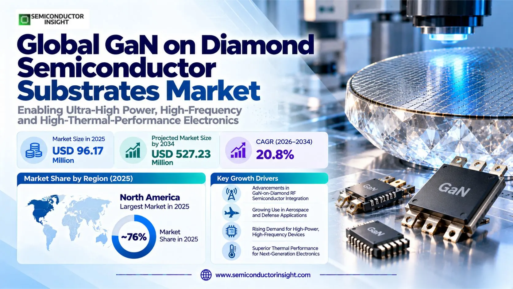
- Market trajectory: the GaN-on-diamond semiconductor substrate market was valued at USD 96.17 million in 2025 and is projected to reach USD 527.23 million by 2034, growing at a CAGR of 20.8% during 2026–2034 as high-power RF devices demand improved near-junction heat removal.
- Four-inch wafers lead the type mix at an estimated ~62% of 2025 revenue, consistent with the established preference for that diameter in available GaN-on-diamond material, while six-inch development formats represent ~9% and carry a modeled ~24.5% growth profile.
- Aerospace and defense represent the largest end-use industry at an estimated ~54% of 2025 demand, reflecting qualification of high-power radar, tactical communication and satellite equipment; RF power amplifiers account for the largest application with an estimated ~36% share.
- North America leads with an estimated ~76% regional share in 2025, ahead of Europe at ~18%, reflecting a concentrated research and specialist supplier ecosystem; the smaller Asia-Pacific market holds ~4% and has a modeled ~23.4% growth rate.
- Thermal interface engineering remains the central commercialization challenge: diamond can dissipate heat rapidly, but bonding quality, thermal boundary resistance, wafer size and high-frequency device reliability determine whether a promising laboratory structure becomes a repeatable production substrate.
GaN on Diamond Semiconductor Substrates Market Overview
GaN on diamond semiconductor substrates market was valued at USD 96.17 million in 2025 and is projected to reach USD 527.23 million by 2034, at a CAGR of 20.8% during 2026–2034. North America is the largest regional market with an estimated ~76% share in 2025, reflecting early work in GaN-on-diamond radio-frequency semiconductor integration and specialized aerospace applications.
GaN-on-diamond semiconductor substrates combine an active gallium nitride device layer with synthetic diamond positioned close to the heat-generating transistor channel. The material architecture addresses a major limitation of high-power RF electronics: concentrated heat can reduce amplifier efficiency and device lifetime even when the GaN transistor itself has attractive electrical properties. Diamond thermal conductivity can exceed 1,500 W/mK in selected grades, but real device performance also depends on the intervening interface and package.
The market includes saleable GaN-on-diamond wafers, bonded or transferred GaN semiconductor layers on diamond, and qualifying pilot or development material supplied for device fabrication. It excludes standalone diamond heat spreaders that contain no GaN, diamond cooling products for GPUs, bare synthetic diamond crystals, and the entire price of a finished radar, satellite radio or amplifier. This boundary matters because many public diamond cooling announcements describe adjacent thermal solutions rather than merchant GaN-on-diamond substrate shipments.
The forecast framework places the 2026 estimate at USD 116.18 million following a 2025 base, with growth extending through 2034. Four-inch material leads with an estimated ~62% of revenue, while two-inch formats account for ~24%, six-inch for ~9%, and specialized dimensions for ~5%. These proportions represent a modeled material mix, not an audited production census. Larger diameters may improve economics, but substrate uniformity and bonding yield can prevent nominal wafer area from translating directly into qualified device output.
High-power radio-frequency applications are the principal source of demand because the thermal advantage is most valuable when device power density is constrained by junction temperature. The 2025 application model assigns ~36% to RF power amplifiers, ~22% to microwave and millimeter-wave circuits, ~17% to radar sensing, ~9% to tactical radios, ~10% to satellite communication equipment, and ~6% to wireless infrastructure. Aerospace and defense end users lead at an estimated ~54%, with telecom and IT at ~29%.
The opportunity remains technically demanding. Transfer processes must remove the original GaN growth substrate without damaging the active layer, create a stable thermal interface to diamond, and retain electrical characteristics after processing. Some approaches grow CVD diamond onto a prepared GaN surface, while others bond an engineered diamond substrate. These pathways differ in equipment, surface preparation and reliability requirements. The most credible growth scenarios depend on successful customer qualification and repeatable material supply rather than theoretical conductivity alone.
Segment Analysis: By Type
By wafer size, the market covers 2-inch, 4-inch, 6-inch and Other formats. Four-inch wafers lead at an estimated ~62% of 2025 revenue and a modeled ~21.2% CAGR. Two-inch substrates contribute ~24% with ~18.4% growth, while six-inch formats account for ~9% and have a faster modeled ~24.5% trajectory as process development explores larger material areas.
| Wafer type | Technical and production role | Market position |
|---|---|---|
| 2-inch Wafers | Two-inch GaN-on-diamond substrates support specialized device research, early wafer transfer and lower-volume RF qualification where process learning matters more than maximum wafer throughput. Smaller material pieces can simplify experimental bonding and inspection, but they do not automatically deliver a low cost per functional transistor. Customers evaluate crystal quality, thermal contact and usable die yield alongside the physical wafer diameter before approving a supplier. | The two-inch category represents an estimated ~24% of 2025 revenue and a modeled ~18.4% CAGR. Its commercial role is concentrated in engineering development, prototypes and specialized production programs. It remains relevant because the highest-priority buyer may need a repeatable high-power device on a small wafer rather than a large substrate that has not yet passed reliability qualification. |
| 4-inch Wafers | Four-inch wafers provide a practical balance between usable area and the handling requirements of specialized GaN-to-diamond integration. The material class is important for customers seeking more repeatable processing without immediately taking on the defect and stress challenges of a larger diameter. Qualification still depends on bonding uniformity, surface flatness and near-junction thermal resistance, not simply the number of die that fit geometrically on the wafer. | The four-inch group holds the largest estimated share at ~62% in 2025, consistent with the publisher’s statement that it exceeds 60%. Its modeled ~21.2% CAGR reflects gradual adoption across qualified RF and aerospace programs. Commercial value arises when a wafer format can move from demonstration to repeatable assembly with stable yields, rather than from a speculative assumption that every RF device will switch substrates. |
| 6-inch Wafers | Six-inch GaN-on-diamond material is a scaling opportunity for suppliers that can maintain transfer quality and interface integrity across a larger area. A larger diameter offers more potential device sites, but it also magnifies challenges in bow, bonding defects and thermal uniformity. Equipment compatibility and inspection become important as processes migrate from laboratory samples toward more industrially repeatable wafer formats. | The six-inch category represents an estimated ~9% of 2025 value and has a modeled ~24.5% CAGR, faster than the established four-inch segment. This outlook reflects potential manufacturing learning rather than an assertion of broad current commercial capacity. Buyers will require convincing yield and reliability evidence before assigning high-volume radar or satellite programs to newly scaled substrate platforms. |
| Other | Other dimensions include special research coupons, nonstandard wafer formats and customized substrate shapes prepared for particular RF devices or thermal test structures. Such material can be essential for experimental near-junction cooling studies, where a small device region matters more than full-wafer compatibility. Pricing and qualification vary widely, so this group cannot be interpreted as a single standardized commodity with interchangeable suppliers. | Specialty formats account for an estimated ~5% of 2025 market revenue and are modeled to grow at ~19.0% through 2034. They can support valuable pilot programs and novel packaging concepts, but limited repeatability restricts broad procurement. The principal market signal is progress toward qualified GaN-on-diamond material that can be transferred into a defined production process. |
Diamond material architecture and end-use segmentation
By diamond type, polycrystalline diamond leads with an estimated ~58% of 2025 value and a modeled ~20.2% CAGR because CVD thermal material is commercially accessible in multiple grades. Single-crystal diamond contributes an estimated ~32% and a modeled ~22.3% CAGR in specialized high-performance uses. Hybrid diamond composites, including diamond combined with SiC or silicon structures, represent ~10%, reflecting engineering routes that balance heat spreading with mechanical or integration constraints.
The end-use segmentation separates Aerospace & Defense at an estimated ~54% of 2025 revenue from IT & Telecommunication at ~29%, Research & Development at ~12%, and other industries at ~5%. Defense and aerospace demand centers on sustained RF power under strict size and reliability limits, whereas research buyers pay for experimental wafers and characterization. The other category includes emerging automotive and healthcare applications without treating complete downstream equipment as substrate sales.
Segment Analysis: By Application
Application demand is divided among RF Power Amplifier, Microwave & Millimeter Wave Circuits, Radar Sensing Equipment, Tactical Radios, Communications Satellite Equipment and Wireless Infrastructure. RF power amplifiers lead with an estimated ~36% of 2025 revenue, while microwave and millimeter-wave circuits contribute ~22% and radar sensing accounts for ~17%.
| Application | Demand characteristics |
|---|---|
| RF Power Amplifier | RF power amplifiers account for an estimated ~36% of 2025 substrate demand and have a modeled ~21.0% CAGR. Their transistors can generate intense localized heat at high output density, making the near-junction thermal path a key design constraint. GaN-on-diamond offers a route to lower operating temperatures, but manufacturers must preserve RF gain, matching and reliability after transfer or diamond growth, and cannot rely on material conductivity alone. |
| Microwave & Millimeter Wave Circuits | Microwave and millimeter-wave circuits represent an estimated ~22% of 2025 revenue and a modeled ~22.1% CAGR. High-frequency operation makes electrical parasitics and local heat removal especially important in compact modules. Engineers need predictable thermal boundary resistance and stable dielectric properties near the device. Substrate suppliers may win specialized sockets when integration improves useful RF output without forcing a complete redesign of the surrounding circuit. |
| Radar Sensing Equipment | Radar sensing applications hold an estimated ~17% of 2025 market value and a modeled ~20.7% CAGR. Phased-array architectures place many power-amplifying channels close together, creating thermal concentration that can constrain output and duty cycle. Diamond-integrated GaN materials are therefore relevant to device research and qualification, but the revenue model counts the qualifying substrate material rather than the entire array, antenna or radar system. |
| Tactical Radios | Tactical radio equipment represents an estimated ~9% of 2025 demand with a modeled ~19.5% CAGR. Portable or vehicle-mounted communications must balance transmitter performance against battery use, weight and thermal headroom. A substrate that lowers the temperature of a GaN amplifier may support a more compact design, but military acceptance also requires ruggedness, traceability and reproducible component behavior across operating environments. |
| Communications Satellite Equipment | Satellite communications equipment contributes an estimated ~10% of 2025 value and a modeled ~22.0% CAGR. Thermal dissipation is challenging in space because convective cooling is absent, making conductive heat paths central to transmitter reliability. GaN-on-diamond integration can be attractive for small high-power radios, although flight heritage and qualification remain prerequisites. The complete satellite payload and radio assembly are excluded from substrate-level revenue. |
| Wireless Infrastructure | Wireless infrastructure represents an estimated ~6% of 2025 revenue and a modeled ~13.2% CAGR, reflecting selective rather than universal adoption. Macro radio and backhaul suppliers already use mature GaN-on-SiC or other RF technologies, so a diamond substrate must demonstrate measurable thermal or power-density benefits before replacing a qualified design. The opportunity is strongest in heat-constrained high-output circuits, not in every base station installed. |
The six application categories differ in qualification cycle and economic value. A defense radar program may pay for a specialized substrate that sustains higher duty cycle, whereas a commercial radio supplier needs reproducible device performance and cost discipline across larger volumes. Satellite electronics prioritize flight heritage and reliable thermal paths. These contrasts explain why the modeled ~36% RF amplifier share is a useful demand signal but cannot be equated with the entire GaN power-amplifier market.
Regional Analysis
North America leads the GaN-on-diamond semiconductor substrate market with an estimated ~76% of 2025 revenue and a modeled ~20.5% CAGR. Europe follows at ~18% and ~20.9%, Asia-Pacific holds ~4% with ~23.4% growth, while South America and the Middle East and Africa each account for ~1%. The distribution reflects concentrated specialist research and qualification rather than the geography of all downstream diamond-cooled electronics.
How does regional commercialization differ for GaN-on-diamond material?
The market is unusually concentrated because GaN-on-diamond integration is not yet a broadly standardized semiconductor manufacturing process. North American activity includes early transistor-transfer research and specialist space-radio applications, while Europe contributes synthetic diamond materials and RF thermal engineering. Asia-Pacific has strong semiconductor and RF capabilities but a smaller modeled share of this specific substrate category. The remaining regions principally encounter the technology through imported defense, communications and industrial systems.
The estimated 2025 regional shares sum to 100%: North America ~76%, Europe ~18%, Asia-Pacific ~4%, South America ~1%, and Middle East and Africa ~1%. The two largest regions therefore represent ~94% of modeled value, consistent with the early-stage concentration of development programs. Higher percentage growth in smaller regions should not be mistaken for a larger absolute opportunity; customer qualification and wafer transfer capability still determine where meaningful substrate revenue can arise.
| Region | Position | Growth outlook | Demand profile | What decides supplier selection |
|---|---|---|---|---|
| North America | Largest (~76%) | Modeled ~20.5% CAGR | Specialist GaN-diamond research and space RF | Transfer process IP, military qualification and substrate repeatability |
| Europe | Second (~18%) | Modeled ~20.9% CAGR | CVD diamond materials and RF thermal engineering | Thermal grade, bonding compatibility and metrology |
| Asia-Pacific | Third (~4%) | Modeled ~23.4% CAGR | Advanced RF design and substrate research | Process access, wafer integration and validation |
| South America | Fourth (~1%) | Modeled ~24.3% CAGR | Imported high-power RF and research systems | Distributor access, cost and equipment qualification |
| Middle East & Africa | Fifth (~1%) | Modeled ~26.3% CAGR | Specialist communications and aerospace projects | Program timing, export rules and lifecycle support |
Competitive Landscape of GaN on Diamond Semiconductor Substrates
The competitive environment is concentrated among specialized GaN-diamond technology developers, synthetic diamond material suppliers and RF semiconductor companies investigating thermal integration. Akash Systems is directly associated with transferred GaN-on-diamond technology; Element Six provides relevant CVD diamond materials; RFHIC has described GaN-to-diamond process work; and Qorvo participates in high-power RF ecosystems. A company’s general GaN or diamond portfolio is not proof of revenue from this exact substrate configuration.
Commercial differentiation begins at the GaN-to-diamond interface. Suppliers must demonstrate that the original growth substrate can be removed or the diamond structure deposited without compromising device operation. Surface flatness, thermal boundary resistance and wafer uniformity matter because even highly conductive bulk diamond cannot compensate for a poorly engineered junction. Intellectual property and reproducible integration steps may therefore be more important than access to generic synthetic diamond feedstock.
Element Six supplies multiple CVD diamond thermal grades, including materials with published conductivity above 1,300 W/mK and above 2,200 W/mK. Those specifications provide an input for thermal engineering but should not be treated as evidence that every diamond product contains a GaN semiconductor layer. The distinction between a diamond heat spreader and a finished GaN-on-diamond wafer is essential when comparing material suppliers with companies that deliver integrated semiconductor structures.
Akash Systems has promoted GaN-on-diamond for high-performance space radios and has expanded its wider Diamond Cooling business into GPU and server products. These developments demonstrate thermal integration capabilities and commercial relationships, but the server products are not necessarily GaN-on-diamond semiconductor substrates. The substrate market should include only the qualifying material or pilot integration revenue, while the full price of a satellite radio, AI server or cooling system belongs to a different product market.
RFHIC has discussed a GaN epitaxial transfer route involving temporary carrier attachment, removal of the original growth substrate, diamond seeding and CVD growth. Its conventional RF transistor and amplifier catalog also prominently features GaN-on-SiC technology. For that reason, the company should be evaluated at the product level rather than assuming all of its RF sales qualify as GaN-on-diamond. Similar caution applies to other semiconductor brands with broad GaN portfolios.
Tier structure
| Tier | Companies | Basis of competition |
|---|---|---|
| Integrated GaN-diamond developer | Akash Systems | A specialist that combines transferred GaN semiconductor layers with synthetic diamond can compete through process intellectual property, near-junction thermal performance and specialized customer qualification. The commercial challenge is converting compelling RF demonstrations into repeatable substrate and device supply. Downstream radio and cooling product sales must be separated from the revenue associated with GaN-on-diamond material itself. |
| Diamond material supplier | Element Six | High-conductivity CVD diamond materials, thermal-grade selection and surface preparation support the substrate integration ecosystem. A supplier in this tier may offer several diamond grades and composite products for unrelated applications, so its total corporate or thermal-management sales do not define the GaN-on-diamond market. Value depends on whether a qualified GaN layer is actually integrated with the material delivered to a device customer. |
| RF integration participants | RFHIC Corporation; Qorvo and selected RF research partners | RF semiconductor companies possess amplifier design, epitaxial device and qualification experience relevant to diamond integration. Their role may include prototypes, process evaluation or specialized development rather than a confirmed merchant wafer line. Conventional GaN-on-SiC transistors and finished RF systems should remain outside the substrate revenue denominator unless a particular GaN-on-diamond material stack is verified. |
Key companies profiled
- Akash Systems
- Element Six
- RFHIC Corporation
- Qorvo
- Selected RF research and device integration partners
Manufacturing Capacity, Wafer Transfer and Process Economics
GaN-on-diamond manufacturing differs from conventional substrate fabrication because the active GaN semiconductor layer must be coupled closely to a synthetic diamond thermal path. Processes may transfer GaN from an original host wafer or deposit diamond onto a prepared device structure. Production readiness depends on interface quality, wafer bow, yield, thermal characterization and repeatable device electrical performance, rather than the availability of bulk diamond alone.
The critical manufacturing sequence begins with a qualified GaN epitaxial layer, followed by surface preparation, original substrate removal or compatible bonding, and formation of a diamond thermal interface. Some flows use a temporary carrier to protect the device side during backside processing. The resulting wafer must survive handling, polishing and device fabrication without introducing defects that erase the expected thermal benefit. Material samples that pass a laboratory test still require scale-up evidence before broad procurement.
Wafer diameter affects potential throughput but also changes mechanical and thermal risks. Four-inch substrates hold an estimated ~62% of the 2025 type market because they provide a workable integration format, while six-inch material represents ~9% and is associated with a faster modeled growth trajectory. A larger wafer can contain more die in principle, yet poor transfer uniformity or a low functional yield can raise rather than lower the cost per qualified RF device.
Testing must evaluate more than bulk thermal conductivity. Thermal boundary resistance between GaN and diamond, electrical behavior after integration, cycling durability and the package heat path all influence device lifetime. The 2025 academic work on diamond heat-sink packaging illustrates why package architecture can change thermal resistance and stress. Such studies are relevant evidence of engineering constraints, but their experimental results should not be presented as market-wide production yields or supplier revenue figures.
Market Dynamics: Drivers, Restraints and Growth Opportunities
GaN-on-diamond adoption is driven by thermal limitations in high-power RF amplifiers, specialized radar and satellite requirements, advances in synthetic diamond materials, and growing experience with transfer or deposition processes. These benefits are offset by bonding complexity, yield uncertainty, device qualification and the availability of established GaN-on-SiC solutions. The market therefore develops through selective high-value applications rather than immediate mass replacement across all radio-frequency equipment.
MARKET DRIVERS
Drivers Impact Analysis*
| Market Drivers | Impact Rank | CAGR Contribution (%) | 2026–2028 | 2029–2031 | 2032–2034 |
|---|---|---|---|---|---|
| High-power RF amplifier thermal limits | High | +7.20% | High | High | High |
| Aerospace and radar power-density requirements | High | +5.80% | High | High | Medium |
| Satellite and microwave integration programs | Medium-High | +4.40% | Medium | High | High |
| CVD diamond material and bonding improvements | Medium | +3.50% | Medium | High | High |
| Four-inch process learning and larger wafer formats | Low-Medium | +2.70% | Medium | High | High |
| Others (specialty research, advanced packaging, device demonstrations) | Low | +1.40% | Low | Medium | Medium |
Thermal headroom enables new RF design choices
High-output GaN transistors can be limited by heat concentrated near the active channel, even when their electrical characteristics permit greater power density. A diamond substrate positioned close to that channel can lower thermal resistance if the interface is engineered well. The modeled ~36% RF amplifier application share reflects this use case, although any actual improvement must be verified in the finished device rather than inferred from diamond conductivity alone.
Radar and aerospace systems value sustained output
A phased-array radar or satellite transmitter may need high RF output in a restricted volume, making heat removal an unusually valuable design attribute. Aerospace and defense account for an estimated ~54% of 2025 end-use demand in the model. Procurement remains qualification-intensive because vibration, temperature cycling and mission lifetime matter, but a successful device-level thermal solution can justify material costs that would be unacceptable in ordinary consumer electronics.
Microwave circuits create concentrated thermal loads
Microwave and millimeter-wave circuits can place active devices and matching structures in compact layouts where thermal and electrical design interact. The estimated ~22% application share is supported by interest in maintaining RF performance at high power density. GaN-on-diamond can provide a new thermal path, but bonding and dielectric characteristics must preserve circuit behavior; a substrate that cools effectively while degrading RF matching will not secure a production design.
Diamond materials continue to diversify
CVD diamond suppliers offer different thermal grades, thicknesses and composite structures that can be selected for specific integration needs. A high-conductivity grade is useful only when its surface and mechanical properties match the GaN transfer or deposition process. This gives materials companies an opportunity to collaborate with device makers on interface engineering, rather than compete solely on a single conductivity number quoted in W/mK.
Process learning can improve wafer economics
Repeatable four-inch material production provides a foundation for evaluating larger wafer formats and reducing defect-related losses. The modeled ~9% six-inch share remains small, but its ~24.5% growth outlook reflects potential improvement in handling, bonding and inspection. Such progress would expand addressable device programs if functional yield improves, while the present market continues to include pilot and development-stage material transactions.
Specialist research sustains early adoption
Universities, defense laboratories and semiconductor research partners investigate thermal boundary resistance and electrical effects at the diamond interface. Their work can identify design rules before commercial customers commit to large orders. Research and development represents an estimated ~12% of the end-use model, indicating that early demand includes materials and prototypes whose value should be distinguished from finished radar or communication systems.
MARKET RESTRAINTS
Restraints Impact Analysis*
| Market Restraints | Impact Rank | CAGR Contribution (%) | 2026–2028 | 2029–2031 | 2032–2034 |
|---|---|---|---|---|---|
| Interface and transfer process complexity | High | -1.80% | High | High | Medium |
| Qualification and wafer-yield uncertainty | Medium-High | -1.20% | High | Medium | Medium |
| Established GaN-on-SiC RF alternatives | Medium | -0.80% | Medium | High | High |
| Others (metrology cost, sourcing limits, customer concentration) | Low | -0.40% | Medium | Medium | Low |
Thermal boundary resistance can erase theoretical gains
Diamond may have very high bulk thermal conductivity, yet a poor bond or interfacial layer can impede heat flow immediately beneath the GaN transistor. Device engineers must characterize the actual near-junction temperature rather than assume that a 2,200 W/mK material automatically produces a proportional system improvement. Transfer damage, surface roughness and unwanted electrical effects can make a nominally attractive wafer unsuitable for production.
Yield and lifetime evidence constrain procurement
Aerospace and defense customers require reproducible electrical performance and reliability over demanding operating conditions. GaN-to-diamond transfer can introduce additional process steps that affect wafer yield, stress and contamination. A specialist supplier may produce impressive prototypes while still lacking the repeatable volume needed for a major qualification program. This delays revenue conversion and increases the cost of testing each new material configuration.
Conventional RF technologies remain competitive
GaN-on-SiC amplifiers have an established commercial base and known design characteristics, so equipment makers do not automatically replace them with diamond-integrated structures. A new substrate must provide a measurable improvement in output power, thermal margin or equipment size after accounting for manufacturing cost and redesign effort. In many radio systems, improved heat sinks or packaging may be sufficient without changing the semiconductor growth substrate.
MARKET OPPORTUNITIES
Repeatable bonded substrates for qualified RF devices
A supplier that can deliver consistent GaN-on-diamond wafers with controlled thermal interfaces may move from research orders into specialized RF device programs. Customers need documented wafer specifications, predictable electrical behavior and reliable handling through downstream processing. The commercial prize is not simply larger wafer diameter but a repeatable material platform that a device manufacturer can qualify without redesigning its entire amplifier architecture.
Thermal engineering partnerships across the value chain
Diamond material companies, GaN epitaxy specialists and RF amplifier manufacturers can collaborate to optimize the entire heat path from transistor channel to package. This is an opportunity because no single bulk material parameter captures device performance. Successful partnerships may create proprietary transfer methods and stronger customer relationships, while retaining a clear distinction between merchant substrate revenue and downstream equipment sales.
Specialized satellite and radar applications
High-value defense and space programs may accept additional material cost when a GaN-on-diamond solution demonstrates sustained RF power in a smaller package. The modeled ~10% satellite application share and ~17% radar share indicate important specialized demand pockets. Suppliers can build qualification histories through these programs before pursuing broader wireless infrastructure markets, where pricing and volume expectations are usually more demanding.
GaN-on-Diamond Semiconductor Substrate Value Chain
The value chain begins with synthetic diamond and GaN epitaxial material, continues through wafer transfer or diamond deposition, and ends with semiconductor device qualification and RF system integration. Material revenue is earned when a qualifying GaN-on-diamond substrate or development wafer is supplied, not when a complete satellite radio or diamond-cooled GPU server is sold. Thermal interface performance connects every stage of this specialized chain.
Upstream materials. CVD diamond suppliers provide material with different thermal conductivity, surface flatness and mechanical characteristics, while GaN epitaxy providers supply the active semiconductor layer. A synthetic diamond wafer without integrated GaN is an upstream input rather than a completed GaN-on-diamond substrate. This distinction matters when a supplier also sells thermal heat spreaders for GPUs, laser packages or other products whose revenue cannot be attributed to this semiconductor category.
Transfer and integration. Integration may require a temporary carrier, removal of the original growth substrate, deposition of diamond seed layers and CVD growth or an alternative bonding process. The most difficult quality attributes include a low-resistance thermal interface and retention of transistor electrical characteristics. Material producers need inspection and process control that can identify defects before expensive RF device fabrication, because the cost of rework rises sharply after further processing.
Device qualification. RF device manufacturers assess channel temperature, power output, gain, stress and reliability after integrating the diamond substrate. The 2025 IEEE thermal packaging research shows that package-level heat removal can materially affect junction-to-case resistance, but its results are not a substitute for GaN-on-diamond wafer yield data. Qualified material must perform in the actual device and package, not only in a stand-alone thermal conductivity measurement.
Downstream equipment. Radar, satellite and communications equipment makers purchase functioning RF systems with defined performance and lifetime requirements. Their qualification decisions influence demand for specialized GaN-on-diamond wafers, yet most of the final equipment price reflects other components, engineering and assembly. A space radio or server cooling contract should therefore be treated as adjacent evidence of thermal technology adoption unless the portion attributable to integrated GaN-on-diamond substrate material is established.
Recent Developments in the GaN on Diamond Semiconductor Substrates Market
- 8 September 2026 Product update
RFHIC outlined its DiaFlux family of polycrystalline CVD diamond thermal materials, with published grades of 1,500 and 1,800 W/mK at 25°C. The announcement demonstrates increasing attention to semiconductor heat-spreading materials and offers useful input specifications for future integration studies. These are diamond thermal products, however, and should not automatically be booked as GaN-on-diamond semiconductor substrates unless a GaN layer is actually integrated. Source - 20 August 2026 Preprint
Researchers published a computational study of diamond heat spreaders around GaN field-effect transistors, identifying an electrostatic trade-off at the diamond interface alongside thermal benefits. The work highlights the need for engineered interlayers and careful electrical characterization rather than relying only on high thermal conductivity. It is a research contribution, not evidence of production revenue or independently audited market size. Source - 3 March 2026 Announced
Akash Systems announced diamond-cooled AMD MI350X GPU servers in collaboration with MiTAC Computing and reported performance claims for its broader Diamond Cooling technology. The development demonstrates commercial interest in synthetic diamond heat removal beyond RF applications. It is deliberately classified as adjacent context because a GPU server cooling product is not the same revenue object as a GaN semiconductor layer transferred to a diamond substrate. Source - 11 September 2025 Published
An IEEE Transactions on Electron Devices paper described experimental diamond heat-sink packaging for GaN HEMTs, including reduced thermal resistance and improved temperature behavior under specified test conditions. The findings support the technical rationale for bringing diamond close to heat-generating devices, while remaining distinct from full-wafer GaN-on-diamond commercialization. Package-level experimental results cannot be substituted for merchant substrate shipment or supplier-share statistics. Source - 22 January 2025 Introduced
Element Six announced a copper-diamond composite aimed at high-performance semiconductor thermal management, including GaN RF applications. The material broadens available packaging options and may complement direct GaN-on-diamond integration where mechanical or thermal requirements differ. Because a copper-diamond composite can be supplied without an active GaN semiconductor layer, the development is relevant competitive context but not direct evidence of qualifying substrate sales. Source - 14 January 2025 Flight milestone
Akash Systems reported that a diamond-cooled satellite radio launched into low Earth orbit with Pixxel, establishing a demanding downstream demonstration for its thermal technology. The milestone is important for customer confidence in space applications, where sustained RF performance and reliable heat paths are essential. The full radio price remains outside the GaN-on-diamond substrate market, whose value is confined to qualifying integrated semiconductor material. Source - 13 November 2024 Proposed funding
Akash Systems announced a non-binding preliminary agreement for proposed CHIPS Act support associated with its diamond cooling activities, including space and semiconductor applications. The proposal illustrates potential support for domestic technology development, but it was not equivalent to a final grant disbursement or recorded GaN-on-diamond substrate sales. Manufacturing investments require separate evidence of process yield, customer qualification and delivered wafer volumes. Source
REPORT SCOPE & SEGMENTATION
| Attribute | Details |
|---|---|
| Study Period | 2020–2034 |
| Base Year | 2025 |
| Estimated Year | 2026 |
| Forecast Period | 2026–2034 |
| Historical Period | 2020–2024 |
| Market Size 2025 | USD 96.17 million |
| Market Size 2026 | USD 116.18 million |
| Market Size 2034 | USD 527.23 million |
| Growth Rate | CAGR of 20.8% during 2026–2034 |
| Units | Revenue in USD million; wafer diameter in inches; thermal conductivity in W/mK |
| Segmentation | By Type, By Diamond Type, By Application, By End-use Industry and By Region |
| By Type | 2-inch Wafers · 4-inch Wafers · 6-inch Wafers · Other |
| By Diamond Type | Single Crystal Diamond · Polycrystalline Diamond · Hybrid Diamond Composites (Diamond + SiC/Si) |
| By Application | RF Power Amplifier · Microwave & Millimeter Wave Circuits · Radar Sensing Equipment · Tactical Radios · Communications Satellite Equipment · Wireless Infrastructure |
| By End-use Industry | Aerospace & Defense · IT & Telecommunication · Research & Development · Others (Automotive, Healthcare, etc.) |
| By Region | Five-region analysis covers Type, Diamond Type, Application, End-use Industry and selected countries North AmericaUnited States, Canada, Mexico EuropeUnited Kingdom, Germany, France, Rest of Europe Asia-PacificSouth Korea, Japan, China, India, Rest of Asia-Pacific South AmericaBrazil, Argentina, Rest of South America Middle East & AfricaUnited Arab Emirates, Saudi Arabia, South Africa, Rest of Middle East & Africa |
| Key Companies Profiled | Akash Systems, Element Six, RFHIC Corporation, Qorvo, specialist GaN epitaxy and diamond integration partners |
| Customization Scope | Additional country and technology coverage can address diamond grade, wafer size, interface architecture, pilot material programs, RF qualification and substrate supplier roles. |
Frequently Asked Questions
What is the current value and forecast of the GaN-on-diamond substrate market?
The global market for GaN-on-diamond semiconductor substrates was valued at USD 96.17 million in 2025 and is projected to reach USD 527.23 million by 2034, reflecting a CAGR of 20.8% during 2026–2034. Demand is linked to specialized RF applications that require improved near-junction thermal performance, while commercialization depends on qualified wafer integration rather than the theoretical conductivity of diamond alone.
What is meant by GaN on diamond?
GaN-on-diamond describes a semiconductor structure in which a gallium nitride device layer is integrated with synthetic diamond so that heat can leave the active transistor region efficiently. Integration may involve transfer from an original growth substrate or deposition of diamond onto a prepared surface. It differs from placing an ordinary diamond heat spreader beneath an unrelated chip, and the revenue boundary depends on that distinction.
Which wafer size accounts for the largest share?
Four-inch GaN-on-diamond wafers lead with an estimated ~62% of 2025 revenue, followed by two-inch formats at ~24%, six-inch material at ~9%, and other specialized sizes at ~5%. The leading position reflects a practical integration format rather than universal standardization. Customers evaluate transfer uniformity, thermal boundary resistance and usable device yield before deciding whether a larger wafer offers a genuine economic advantage.
Which diamond material type is most significant?
Polycrystalline diamond holds an estimated ~58% of the 2025 diamond-type mix, reflecting the availability of CVD thermal material for engineered integration. Single-crystal diamond accounts for roughly ~32%, while hybrid diamond composites represent ~10%. Each architecture has different implications for crystal quality, bonding, stress and thermal performance, so the best material choice depends on the specific GaN device and package rather than a single bulk conductivity rating.
Which region leads GaN-on-diamond commercialization?
North America leads with an estimated ~76% of 2025 revenue, supported by early transfer-process research and specialist high-power RF applications. Europe follows with roughly ~18% through diamond materials and thermal engineering capabilities. Asia-Pacific contributes ~4%, while South America and the Middle East and Africa each account for ~1%. These shares are a modeled allocation of substrate revenue, not a distribution of all downstream diamond-cooled electronics.
What are the largest applications for GaN-on-diamond?
RF power amplifiers represent an estimated ~36% of 2025 demand, followed by microwave and millimeter-wave circuits at ~22% and radar sensing at ~17%. Tactical radios, satellite communication equipment and wireless infrastructure comprise smaller application groups. The thermal benefit is most relevant where a transistor operates near a sustained power-density limit, but qualifying a new substrate also requires electrical and lifetime testing.
Why are aerospace and defense customers important?
Aerospace and defense account for an estimated ~54% of 2025 end-use demand because high-power radar and space communications can value thermal margin, compact size and sustained RF output. These customers also require demanding qualification, which can extend development timelines. A material supplier may gain from pilot or specialized production orders before broader adoption, but the entire price of a radar or satellite payload remains outside substrate revenue.
What prevents rapid mass-market adoption?
The principal barriers are wafer transfer complexity, thermal interface resistance, low or uncertain yield, device reliability and the availability of established GaN-on-SiC alternatives. Diamond can conduct heat rapidly in bulk form, but an imperfect interface can limit the practical benefit. Suppliers must demonstrate stable transistor electrical performance and repeatable manufacturing before customers commit high-volume designs, particularly in safety-critical RF equipment.
Which companies participate in this technology?
Akash Systems is associated with GaN-on-diamond integration and space-radio applications; Element Six provides synthetic diamond thermal materials; RFHIC has discussed relevant epitaxial transfer work; and Qorvo participates in the broader high-power RF ecosystem. Their product scopes differ, so no total corporate revenue or generic GaN amplifier sales should be treated automatically as merchant GaN-on-diamond substrate revenue.
Are diamond-cooled GPU servers included in the market?
Diamond-cooled GPU servers and general-purpose heat spreaders are excluded unless they contain a qualifying GaN semiconductor layer integrated with diamond and the relevant material revenue can be identified. The commercial success of diamond cooling in computing is useful adjacent evidence of thermal-material capability, but a server contract cannot be substituted for sales of GaN-on-diamond wafers. The distinction prevents mixing component, materials and equipment markets.
Research Sources & Evidence Base
Get Sample Report PDF for Exclusive Insights
Report Sample Includes
- Table of Contents
- List of Tables & Figures
- Charts, Research Methodology, and more...
 Download Sample Report PDF