SEMICONDUCTOR INSIGHT
MARKET RESEARCH REPORT

Gallium Nitride (GaN) Wafer Foundry Market

2026 to 2034
MARKET INTELLIGENCE
ACROSS KEY REGIONS
2026 EDITION
SEMICONDUCTOR FOUNDRY SERVICES / POWER ELECTRONICS / RF / WIDE BANDGAP Semiconductor Market Research

Gallium Nitride (GaN) Wafer Foundry Market

Size, Share & Industry Analysis, By Type (GaN-on-Si Wafer Foundry, GaN-on-SiC Wafer Foundry), By Application (GaN Power Devices, GaN RF Devices, Optoelectronics, Others), By End User (Telecommunications, Aerospace & Defense, Automotive, Consumer Electronics), By Wafer Size (4-inch Wafers, 6-inch Wafers, 8-inch Wafers), By Production Process (MOCVD, MBE, HVPE), and Regional Forecast, 2026-2034

◷
UPDATED 30 October 2026
▤
REPORT LENGTH Detailed Report
▣
REPORT CODE ced904935482
▯
FORMATS PDF

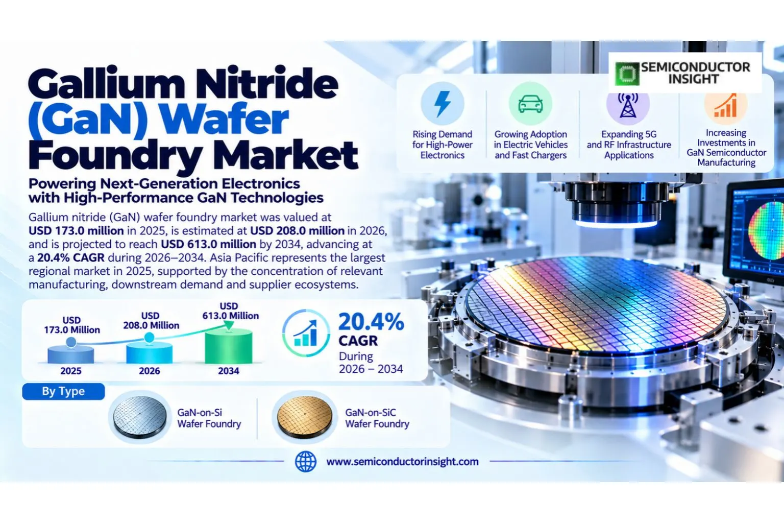
Global gallium nitride (gan) wafer foundry market was valued at USD 173.0 million in 2025, is estimated at USD 208.0 million in 2026, and is projected to reach USD 613.0 million by 2034, advancing at a 20.4% CAGR during 2026–2034. Asia Pacific represents the largest regional market in 2025, supported by the concentration of relevant manufacturing, downstream demand and supplier ecosystems.

Get the sample PDF with study scope, segmentation and methodology details.

Key Statistics

2025 Market Size
USD 173.0 million
2034 Projected Market Size
USD 613.0 million
CAGR (2026–2034)
20.4%
Largest Market in 2025
Asia Pacific

Key Takeaways

  • The global gallium nitride (gan) wafer foundry market was valued at USD 173.0 million in 2025 and is projected to reach USD 613.0 million by 2034, representing a 20.4% CAGR over 2026–2034.
  • GaN-on-Si foundry services are expanding because silicon substrates support larger wafer formats and greater compatibility with established semiconductor infrastructure, while GaN-on-SiC remains important for high-power RF performance.
  • Power electronics and RF infrastructure are the two main demand engines, with electric-vehicle power conversion, data-center power, telecom infrastructure and defense electronics requiring higher efficiency or higher-frequency operation.
  • Asia Pacific leads because Taiwan, South Korea, Japan and China combine compound-semiconductor manufacturing, foundry infrastructure, packaging capability and the largest electronics production base.
  • The transition toward 8-inch GaN-on-Si platforms is strategically important because larger wafer formats improve manufacturing scale and can make outsourced GaN production more accessible to fabless power-device companies.

Gallium Nitride (GaN) Wafer Foundry Market Overview

Gallium nitride (gan) wafer foundry market was valued at USD 173.0 million in 2025, is estimated at USD 208.0 million in 2026, and is projected to reach USD 613.0 million by 2034, advancing at a 20.4% CAGR during 2026–2034. Asia Pacific represents the largest regional market in 2025, supported by the concentration of relevant manufacturing, downstream demand and supplier ecosystems.

Base year: 2025 · Estimated year: 2026 · Forecast period: 2026–2034 · Values in USD million unless otherwise stated

Gallium nitride wafer foundry services provide outsourced fabrication for GaN power, RF and optoelectronic devices using process platforms such as GaN-on-silicon and GaN-on-silicon-carbide. The foundry model lets fabless companies access epitaxy-compatible processing, lithography, etch, metallization, passivation, testing and process-design kits without building dedicated compound-semiconductor fabs. Commercial success depends on device performance, yield, wafer size, process reliability and the foundry’s ability to support customer-specific device architectures.

GaN demand is broadening beyond RF power amplifiers into data-center power conversion, consumer fast charging, electric vehicles and industrial power systems. That shift increases the value of 200 mm GaN-on-silicon capacity because it can leverage more standardized fab infrastructure, while GaN-on-SiC remains favored for high-frequency and high-power RF applications where thermal performance and power density justify higher substrate cost.

The commercial structure of the gallium nitride (gan) wafer foundry market is shaped by design qualification, production economics and the interaction between component performance and downstream system requirements. Suppliers that can combine consistent manufacturing, application engineering and supply assurance are better positioned to convert technical eligibility into repeat business. Customer decisions increasingly account for lifecycle continuity, geographic resilience and integration cost, which makes proven process control and ecosystem compatibility as important as nominal product capability.

Segment Analysis: By Type

By type, the Gallium Nitride (GaN) Wafer Foundry market is segmented into GaN-on-Si Wafer Foundry, GaN-on-SiC Wafer Foundry. GaN-on-Si is the volume-oriented path because it supports larger wafers and leverages silicon-fab infrastructure, while GaN-on-SiC is differentiated by superior thermal conductivity and RF performance. Foundries increasingly position these platforms for different customer economics rather than treating them as direct substitutes. Purchasing decisions vary by performance requirement, qualification burden, integration complexity and lifecycle economics, so suppliers compete on application fit rather than on a single technical specification.

Type Role in the market Demand characteristics
GaN-on-Si Wafer Foundry GaN-on-Si Wafer Foundry addresses a distinct part of the product and process mix. Its commercial position depends on technical fit, manufacturing maturity, integration requirements and customer qualification rather than on headline specifications alone. Demand is strongest where the segment aligns with established customer designs, predictable supply, and measurable system-level performance. Suppliers that can document repeatability, compatibility and lifecycle support are better placed to defend design wins.
GaN-on-SiC Wafer Foundry GaN-on-SiC Wafer Foundry addresses a distinct part of the product and process mix. Its commercial position depends on technical fit, manufacturing maturity, integration requirements and customer qualification rather than on headline specifications alone. Demand is strongest where the segment aligns with established customer designs, predictable supply, and measurable system-level performance. Suppliers that can document repeatability, compatibility and lifecycle support are better placed to defend design wins.

Segment Analysis: By End User

By end user, the Gallium Nitride (GaN) Wafer Foundry market is segmented into Telecommunications, Aerospace & Defense, Automotive, Consumer Electronics. Telecommunications and aerospace/defense remain important for RF GaN, while automotive and consumer-electronics customers are broadening demand for power GaN. Each end-user group has different qualification, reliability and lifecycle expectations. Purchasing decisions vary by performance requirement, qualification burden, integration complexity and lifecycle economics, so suppliers compete on application fit rather than on a single technical specification.

End User Role in the market Demand characteristics
Telecommunications Telecommunications represents a relevant purchasing and deployment pathway within this market. Commercial attractiveness depends on how well it aligns with customer architecture, supply-chain constraints and required performance. Growth is linked to design-in activity, installed-base transitions and the ability of suppliers to meet qualification, cost and availability requirements over the full product lifecycle.
Aerospace & Defense Aerospace & Defense represents a relevant purchasing and deployment pathway within this market. Commercial attractiveness depends on how well it aligns with customer architecture, supply-chain constraints and required performance. Growth is linked to design-in activity, installed-base transitions and the ability of suppliers to meet qualification, cost and availability requirements over the full product lifecycle.
Automotive Automotive represents a relevant purchasing and deployment pathway within this market. Commercial attractiveness depends on how well it aligns with customer architecture, supply-chain constraints and required performance. Growth is linked to design-in activity, installed-base transitions and the ability of suppliers to meet qualification, cost and availability requirements over the full product lifecycle.
Consumer Electronics Consumer Electronics represents a relevant purchasing and deployment pathway within this market. Commercial attractiveness depends on how well it aligns with customer architecture, supply-chain constraints and required performance. Growth is linked to design-in activity, installed-base transitions and the ability of suppliers to meet qualification, cost and availability requirements over the full product lifecycle.

Segment Analysis: By Application

By application, the Gallium Nitride (GaN) Wafer Foundry market is segmented into GaN Power Devices, GaN RF Devices, Optoelectronics, Others. GaN power devices are benefiting from high-frequency switching in data-center power, consumer adapters and automotive conversion, while RF devices remain essential in telecom, radar and defense. Foundry demand therefore spans both high-volume commercial programs and lower-volume, high-value RF designs. Purchasing decisions vary by performance requirement, qualification burden, integration complexity and lifecycle economics, so suppliers compete on application fit rather than on a single technical specification.

Application Role in the market Demand characteristics
GaN Power Devices GaN Power Devices creates demand when the underlying system requires the market’s core function at production scale. Procurement is normally tied to platform launches, equipment upgrades, capacity expansion or replacement cycles. Buyers evaluate reliability, qualification time, integration cost and vendor support alongside unit economics. Adoption accelerates when the solution removes a system bottleneck or supports a new performance tier without creating disproportionate redesign risk.
GaN RF Devices GaN RF Devices creates demand when the underlying system requires the market’s core function at production scale. Procurement is normally tied to platform launches, equipment upgrades, capacity expansion or replacement cycles. Buyers evaluate reliability, qualification time, integration cost and vendor support alongside unit economics. Adoption accelerates when the solution removes a system bottleneck or supports a new performance tier without creating disproportionate redesign risk.
Optoelectronics Optoelectronics creates demand when the underlying system requires the market’s core function at production scale. Procurement is normally tied to platform launches, equipment upgrades, capacity expansion or replacement cycles. Buyers evaluate reliability, qualification time, integration cost and vendor support alongside unit economics. Adoption accelerates when the solution removes a system bottleneck or supports a new performance tier without creating disproportionate redesign risk.
Others Others creates demand when the underlying system requires the market’s core function at production scale. Procurement is normally tied to platform launches, equipment upgrades, capacity expansion or replacement cycles. Buyers evaluate reliability, qualification time, integration cost and vendor support alongside unit economics. Adoption accelerates when the solution removes a system bottleneck or supports a new performance tier without creating disproportionate redesign risk.

Segment Analysis: By Wafer Size

By wafer size, the Gallium Nitride (GaN) Wafer Foundry market is segmented into 4-inch Wafers, 6-inch Wafers, 8-inch Wafers. 6-inch remains widely used across RF and specialty power processes, while 8-inch GaN-on-Si is gaining strategic importance for scalable power-device manufacturing. 4-inch lines remain relevant in specialty and legacy programs. Purchasing decisions vary by performance requirement, qualification burden, integration complexity and lifecycle economics, so suppliers compete on application fit rather than on a single technical specification.

Wafer Size Role in the market Demand characteristics
4-inch Wafers 4-inch Wafers represents a relevant purchasing and deployment pathway within this market. Commercial attractiveness depends on how well it aligns with customer architecture, supply-chain constraints and required performance. Growth is linked to design-in activity, installed-base transitions and the ability of suppliers to meet qualification, cost and availability requirements over the full product lifecycle.
6-inch Wafers 6-inch Wafers represents a relevant purchasing and deployment pathway within this market. Commercial attractiveness depends on how well it aligns with customer architecture, supply-chain constraints and required performance. Growth is linked to design-in activity, installed-base transitions and the ability of suppliers to meet qualification, cost and availability requirements over the full product lifecycle.
8-inch Wafers 8-inch Wafers represents a relevant purchasing and deployment pathway within this market. Commercial attractiveness depends on how well it aligns with customer architecture, supply-chain constraints and required performance. Growth is linked to design-in activity, installed-base transitions and the ability of suppliers to meet qualification, cost and availability requirements over the full product lifecycle.

Segment Analysis: By Production Process

By production process, the Gallium Nitride (GaN) Wafer Foundry market is segmented into MOCVD, MBE, HVPE. MOCVD dominates commercial epitaxy because it supports high-volume, uniform GaN layer growth. MBE and HVPE retain specialized roles where material quality, research flexibility or thick-film growth requirements justify different economics. Purchasing decisions vary by performance requirement, qualification burden, integration complexity and lifecycle economics, so suppliers compete on application fit rather than on a single technical specification.

Production Process Role in the market Demand characteristics
MOCVD MOCVD represents a relevant purchasing and deployment pathway within this market. Commercial attractiveness depends on how well it aligns with customer architecture, supply-chain constraints and required performance. Growth is linked to design-in activity, installed-base transitions and the ability of suppliers to meet qualification, cost and availability requirements over the full product lifecycle.
MBE MBE represents a relevant purchasing and deployment pathway within this market. Commercial attractiveness depends on how well it aligns with customer architecture, supply-chain constraints and required performance. Growth is linked to design-in activity, installed-base transitions and the ability of suppliers to meet qualification, cost and availability requirements over the full product lifecycle.
HVPE HVPE represents a relevant purchasing and deployment pathway within this market. Commercial attractiveness depends on how well it aligns with customer architecture, supply-chain constraints and required performance. Growth is linked to design-in activity, installed-base transitions and the ability of suppliers to meet qualification, cost and availability requirements over the full product lifecycle.

Regional Analysis

Asia Pacific leads the gallium nitride (gan) wafer foundry market in 2025, while regional growth patterns differ according to manufacturing concentration, customer investment cycles, regulation, product mix and supply-chain access. The most important regional distinction is not simply market size; it is the mechanism that converts local investment and end-market demand into qualified purchases.

How does regional demand differ across the gallium nitride (gan) wafer foundry market?

Regional demand for gallium nitride (gan) wafer foundry is structurally uneven because manufacturing assets, design centers, downstream customers and qualification ecosystems are not distributed evenly. Asia Pacific typically has the deepest electronics manufacturing base, North America combines technology development with capital investment, Europe emphasizes reliability and industrial requirements, and emerging regions are more dependent on imported systems. These differences influence vendor selection, inventory policy, service expectations and the pace at which new technologies are adopted.

Region Market position Growth outlook Demand profile Supplier-selection gate
Asia Pacific Largest Very strong Foundry and electronics-manufacturing led Qualified process platforms and capacity
North America High-value demand Strong Power, defense and data-center led Technology access and secure supply
Europe Emerging foundry hub Strong Automotive, industrial and regionalization led Automotive qualification and scalable 200mm capacity
South America Early-stage demand Selective Imported-device led Cost and channel availability
Middle East & Africa Developing Selective Telecom, defense and energy led Project qualification and imported supply

Detailed Regional Blocks

Asia Pacific LARGEST MARKET

What defines the Asia Pacific gallium nitride (gan) wafer foundry market?

Asia Pacific leads the GaN wafer foundry market because Taiwan, South Korea, China and Japan combine compound-semiconductor expertise with dense electronics manufacturing and packaging ecosystems. The region contains major pure-play and specialty foundries, RF manufacturing clusters and fast-growing power-electronics demand, making it the center of both customer qualification and commercial scale-up.

Market positionLargest
Growth outlookVery strong
Demand profileFoundry and electronics-manufacturing led
Market access gateQualified process platforms and capacity
Country / subregion Role Demand logic
Taiwan Foundry center WIN, UMC, TSMC-linked ecosystems and specialty foundry infrastructure support RF and power programs.
China Localization and scale Domestic EV, telecom and power-electronics demand supports GaN investment and local foundry expansion.
South Korea Power and electronics ecosystem Consumer electronics, automotive and semiconductor manufacturing support GaN commercialization.
Japan Materials and device expertise Advanced materials, power electronics and industrial customers create specialized GaN demand.

Market instances

WIN Semiconductors announced in June 2026 that its 0.12 μm NP12-0B GaN-on-SiC process had been qualified for 40 V operation, extending the platform for high-power amplifiers, switches and low-noise amplifiers. The qualification shows continuing investment in RF GaN foundry capability for multifunction front-end designs. For suppliers in Asia Pacific, the commercial implication is a stronger need to align product qualification, account coverage and inventory planning with the local demand mechanism rather than relying on broad global growth assumptions.

WIN’s foundry-service portfolio includes GaN alongside GaAs processes for MMIC applications, supported by 24/7 manufacturing and on-wafer testing. This matters because customers value a stable outsourced path from design support through production and RF test rather than only access to a device recipe. For suppliers in Asia Pacific, the commercial implication is a stronger need to align product qualification, account coverage and inventory planning with the local demand mechanism rather than relying on broad global growth assumptions.

Asian electronics and telecom supply chains shorten the distance between GaN device design, wafer fabrication, packaging and system qualification. That proximity helps suppliers accelerate yield learning and adjust process windows as device architectures move into higher frequencies and higher switching power. For suppliers in Asia Pacific, the commercial implication is a stronger need to align product qualification, account coverage and inventory planning with the local demand mechanism rather than relying on broad global growth assumptions.

Full-report coverage for Asia Pacific examines country-level demand, customer concentration, supplier positioning and the technical or commercial requirements that influence qualification. The regional view is designed to distinguish structural demand drivers from short-lived purchasing cycles and to show where market access depends on local manufacturing, distribution, standards, service capability or long-term customer relationships.

North America HIGH-VALUE DEMAND

What defines the North America gallium nitride (gan) wafer foundry market?

North America is a high-value GaN market driven by defense RF, data-center power, satellite communications, EV power conversion and advanced electronics. The region’s strategic interest in wide-bandgap semiconductors supports domestic capability, while customers place strong weight on trusted manufacturing, long-term supply and device-level performance. Supplier strategies therefore need to reflect local qualification practices, channel structure, end-market priorities and the availability of technically comparable alternatives rather than treating the region as a uniform extension of global demand.

Market positionHigh-value demand
Growth outlookStrong
Demand profilePower, defense and data-center led
Market access gateTechnology access and secure supply
Country / subregion Role Demand logic
United States Defense and data-center demand RF systems, hyperscale power and semiconductor investment create strong GaN pull.
Canada Research and power electronics University and industrial programs support niche device development.
Mexico Automotive adjacency Vehicle and electronics manufacturing can support downstream GaN power adoption.

Market instances

MACOM highlighted GaN foundry services at IMS 2025, covering design assistance, scalable device models, production-ready processes and quality testing. The offering shows how U.S.-based compound-semiconductor suppliers compete on end-to-end support rather than wafer processing alone. For suppliers in North America, the commercial implication is a stronger need to align product qualification, account coverage and inventory planning with the local demand mechanism rather than relying on broad global growth assumptions.

North American data-center expansion increases the value of efficient high-frequency power conversion, creating a long-term route for GaN power devices as server racks and AI accelerators push power density higher. For suppliers in North America, the commercial implication is a stronger need to align product qualification, account coverage and inventory planning with the local demand mechanism rather than relying on broad global growth assumptions.

Defense and aerospace customers continue to require high-power, high-frequency RF components for radar, electronic warfare and satellite systems, supporting specialized GaN-on-SiC processes even where volumes are smaller than commercial power applications. For suppliers in North America, the commercial implication is a stronger need to align product qualification, account coverage and inventory planning with the local demand mechanism rather than relying on broad global growth assumptions.

Full-report coverage for North America examines country-level demand, customer concentration, supplier positioning and the technical or commercial requirements that influence qualification. The regional view is designed to distinguish structural demand drivers from short-lived purchasing cycles and to show where market access depends on local manufacturing, distribution, standards, service capability or long-term customer relationships.

Europe EMERGING FOUNDRY HUB

What defines the Europe gallium nitride (gan) wafer foundry market?

Europe is strengthening its GaN foundry position around power electronics, automotive qualification and supply-chain regionalization. The region is especially relevant for 200 mm GaN-on-silicon platforms that can fit established specialty fabs and give fabless power-device companies an outsourced path to production without relying entirely on Asian capacity. Supplier strategies therefore need to reflect local qualification practices, channel structure, end-market priorities and the availability of technically comparable alternatives rather than treating the region as a uniform extension of global demand.

Market positionEmerging foundry hub
Growth outlookStrong
Demand profileAutomotive, industrial and regionalization led
Market access gateAutomotive qualification and scalable 200mm capacity
Country / subregion Role Demand logic
Germany 8-inch GaN-on-Si manufacturing X-FAB’s Dresden fab supports GaN-on-Si foundry services in an automotive-qualified environment.
Belgium Materials and foundry development X-FAB and regional compound-semiconductor activity support platform development.
France Industrial and defense demand Power electronics and aerospace applications create high-reliability demand.

Market instances

X-FAB launched GaN-on-Si foundry services in September 2025 on its XG035 depletion-mode platform from an 8-inch fab in Dresden. Open MPW, prototyping and production access lowers the entry barrier for fabless GaN companies and strengthens Europe’s outsourced power-semiconductor supply chain. For suppliers in Europe, the commercial implication is a stronger need to align product qualification, account coverage and inventory planning with the local demand mechanism rather than relying on broad global growth assumptions.

In April 2025, IQE and X-FAB announced a two-year joint development agreement for a 650 V GaN power-device platform aimed at automotive, data-center and consumer applications. The collaboration combines epitaxy and foundry processing to create a more standardized route from wafer material to manufacturable device. For suppliers in Europe, the commercial implication is a stronger need to align product qualification, account coverage and inventory planning with the local demand mechanism rather than relying on broad global growth assumptions.

European automotive customers value long qualification cycles, stable process control and regional supply. These requirements can favor foundries that already operate automotive-qualified mixed-signal or power-semiconductor fabs and can integrate GaN into established quality systems. For suppliers in Europe, the commercial implication is a stronger need to align product qualification, account coverage and inventory planning with the local demand mechanism rather than relying on broad global growth assumptions.

Full-report coverage for Europe examines country-level demand, customer concentration, supplier positioning and the technical or commercial requirements that influence qualification. The regional view is designed to distinguish structural demand drivers from short-lived purchasing cycles and to show where market access depends on local manufacturing, distribution, standards, service capability or long-term customer relationships.

South America EARLY-STAGE DEMAND

What defines the South America gallium nitride (gan) wafer foundry market?

South America remains primarily a downstream GaN demand market rather than a wafer-fabrication center. Adoption is linked to EV charging, industrial power conversion, telecom infrastructure and renewable-energy systems, with most devices imported through global semiconductor and equipment supply chains. Supplier strategies therefore need to reflect local qualification practices, channel structure, end-market priorities and the availability of technically comparable alternatives rather than treating the region as a uniform extension of global demand.

Market positionEarly-stage demand
Growth outlookSelective
Demand profileImported-device led
Market access gateCost and channel availability
Country / subregion Role Demand logic
Brazil Largest regional demand base Telecom, industrial electronics and renewable energy support power and RF demand.
Argentina Selective industrial use Industrial and energy applications create smaller GaN opportunities.
Other markets Project driven GaN enters mainly through imported chargers, inverters, telecom systems and power modules.

Market instances

Brazil’s telecom and renewable-energy investment creates demand for high-efficiency power conversion and RF infrastructure even though front-end GaN fabrication is limited. For suppliers in South America, the commercial implication is a stronger need to align product qualification, account coverage and inventory planning with the local demand mechanism rather than relying on broad global growth assumptions.

Imported GaN devices compete against mature silicon and silicon-carbide alternatives, so adoption depends on system-level efficiency, size and thermal advantages being large enough to justify premium component cost. For suppliers in South America, the commercial implication is a stronger need to align product qualification, account coverage and inventory planning with the local demand mechanism rather than relying on broad global growth assumptions.

Regional market access is mostly indirect through module suppliers, telecom equipment vendors and power-electronics integrators rather than through local wafer-foundry relationships. For suppliers in South America, the commercial implication is a stronger need to align product qualification, account coverage and inventory planning with the local demand mechanism rather than relying on broad global growth assumptions.

Full-report coverage for South America examines country-level demand, customer concentration, supplier positioning and the technical or commercial requirements that influence qualification. The regional view is designed to distinguish structural demand drivers from short-lived purchasing cycles and to show where market access depends on local manufacturing, distribution, standards, service capability or long-term customer relationships.

Middle East & Africa DEVELOPING

What defines the Middle East & Africa gallium nitride (gan) wafer foundry market?

Middle East and Africa demand is developing through telecom infrastructure, defense electronics, renewable-energy projects and high-efficiency power systems. Most GaN wafers and devices are imported, but project economics can favor GaN where power density, RF efficiency or thermal performance directly reduce system size and operating cost. Supplier strategies therefore need to reflect local qualification practices, channel structure, end-market priorities and the availability of technically comparable alternatives rather than treating the region as a uniform extension of global demand.

Market positionDeveloping
Growth outlookSelective
Demand profileTelecom, defense and energy led
Market access gateProject qualification and imported supply
Country / subregion Role Demand logic
Gulf Cooperation Council Telecom and defense demand 5G infrastructure, radar and high-value electronics create focused GaN opportunities.
Israel RF and defense ecosystem Advanced RF design and defense electronics support specialized GaN device demand.
South Africa Industrial and telecom demand Industrial power and communications create smaller but technically relevant demand.

Market instances

Telecom densification in Gulf markets raises the value of efficient RF power devices, particularly where base-station footprint and energy consumption are important operating costs. For suppliers in Middle East & Africa, the commercial implication is a stronger need to align product qualification, account coverage and inventory planning with the local demand mechanism rather than relying on broad global growth assumptions.

Defense and aerospace programs favor high-power GaN RF technology because it supports radar, electronic-warfare and satellite systems requiring high frequency and power density. For suppliers in Middle East & Africa, the commercial implication is a stronger need to align product qualification, account coverage and inventory planning with the local demand mechanism rather than relying on broad global growth assumptions.

Renewable-energy and data-center projects create additional demand for high-efficiency power conversion, although wafer-foundry value is captured mainly outside the region. For suppliers in Middle East & Africa, the commercial implication is a stronger need to align product qualification, account coverage and inventory planning with the local demand mechanism rather than relying on broad global growth assumptions.

Full-report coverage for Middle East & Africa examines country-level demand, customer concentration, supplier positioning and the technical or commercial requirements that influence qualification. The regional view is designed to distinguish structural demand drivers from short-lived purchasing cycles and to show where market access depends on local manufacturing, distribution, standards, service capability or long-term customer relationships.

Competitive Landscape

Competition in the gallium nitride (gan) wafer foundry market is determined by technical qualification, manufacturing consistency, customer relationships and the ability to support product lifecycles. Price matters, but it rarely overrides reliability, integration effort or switching cost once a supplier has been designed into a production platform.

The competitive field includes TSMC, GlobalFoundries, United Microelectronics Corporation (UMC), VIS, X-FAB, WIN Semiconductors, alongside other specialized suppliers. Market share can shift when a vendor gains access to a new platform, expands qualified capacity or introduces a technology that materially improves system performance. Because customer validation can be lengthy, incumbent suppliers often benefit from continuity, while challengers need a clear technical or supply-chain advantage to displace an approved source.

Competitive strategy is increasingly multi-dimensional. Leading suppliers invest in process or product development, application engineering and regional support at the same time, while customers seek second-source options where technically feasible. This creates a market in which differentiation is sustained through documented performance, manufacturing yield, quality systems, responsiveness and the ability to support future roadmap transitions without forcing unnecessary redesigns.

Company Competitive position Primary basis of competition
TSMC Established global / strategic supplier Competes through product capability, qualification, account access and supply execution.
GlobalFoundries Established global / strategic supplier Competes through product capability, qualification, account access and supply execution.
United Microelectronics Corporation (UMC) Established global / strategic supplier Competes through product capability, qualification, account access and supply execution.
VIS Established global / strategic supplier Competes through product capability, qualification, account access and supply execution.
X-FAB Established global / strategic supplier Competes through product capability, qualification, account access and supply execution.
WIN Semiconductors Specialist / regional competitor Competes through product capability, qualification, account access and supply execution.
Episil Technology Specialist / regional competitor Competes through product capability, qualification, account access and supply execution.
Chengdu Hiwafer Semiconductor Specialist / regional competitor Competes through product capability, qualification, account access and supply execution.
UMS RF Specialist / regional competitor Competes through product capability, qualification, account access and supply execution.
Sanan IC Specialist / regional competitor Competes through product capability, qualification, account access and supply execution.
Global Communication Semiconductors Focused challenger / niche participant Competes through product capability, qualification, account access and supply execution.
MACOM Focused challenger / niche participant Competes through product capability, qualification, account access and supply execution.
BelGaN Focused challenger / niche participant Competes through product capability, qualification, account access and supply execution.
DB HiTek Focused challenger / niche participant Competes through product capability, qualification, account access and supply execution.
Samsung Electronics Focused challenger / niche participant Competes through product capability, qualification, account access and supply execution.

Production Capacity Analysis

GaN foundry capacity must be assessed by qualified process platform rather than wafer diameter alone. Epitaxy source, substrate type, gate structure, voltage class, RF model accuracy and reliability qualification determine whether a fab can serve a specific design. Capacity that is technically available for one GaN application may not be interchangeable with another without substantial process development.

The industry is expanding from 4-inch and 6-inch specialty lines toward 8-inch GaN-on-Si for power applications. X-FAB’s Dresden platform illustrates this shift, while RF GaN remains strongly associated with GaN-on-SiC and compound-semiconductor fabs such as WIN and MACOM. The resulting market is likely to retain multiple process architectures rather than converging immediately on one wafer format.

Capacity should therefore be evaluated on a qualified-output basis rather than as nominal installed capability. A supplier may possess equipment or production lines that appear suitable but still require customer-specific validation, process tuning, test correlation or upstream material qualification. This distinction becomes especially important during demand spikes, when headline capacity can overstate the volume that is immediately available for a particular application, technology generation or reliability class.

Market Dynamics

The gallium nitride (gan) wafer foundry market is being shaped by rising performance requirements and technology transitions on the demand side, while qualification complexity, supply concentration and cost discipline constrain the pace of adoption. The balance of these forces favors suppliers that can solve a measurable system problem without increasing integration risk.

Demand expansion is not uniform across all product variants or customer groups. New technology creates attractive design opportunities, but buyers typically require a clear economic or performance case before changing a qualified architecture. At the same time, supply-chain localization, capacity investment and tighter quality requirements are changing procurement behavior. As a result, growth is likely to concentrate around applications where performance upgrades, manufacturing scale and lifecycle value reinforce one another.

Market Drivers

Four forces provide the strongest support for demand in the gallium nitride (gan) wafer foundry market: performance-driven technology upgrades, expansion of relevant downstream applications, investment in manufacturing or infrastructure, and the need for more resilient supply. Their importance varies by segment, but each creates a direct reason for customers to qualify or purchase additional solutions.

Driver Impact Commercial mechanism
High-frequency power conversion is moving beyond silicon High GaN enables faster switching and lower losses in chargers, servers and industrial power systems. As power density rises, device makers need foundries with mature GaN process design kits, gate reliability and production yield.
5G, radar and satellite systems sustain RF GaN demand High GaN-on-SiC delivers high power density and frequency performance for base stations, radar, electronic warfare and satellite communications, supporting specialized foundry programs with demanding reliability requirements.
200 mm GaN-on-Si improves manufacturing economics Medium-High Larger wafers and compatibility with established silicon equipment can reduce cost per die and expand capacity. This is encouraging specialty foundries to add 8-inch GaN platforms and MPW access.
Regional semiconductor policy supports outsourced wide-bandgap capacity Medium-High Governments and industrial customers increasingly want resilient semiconductor supply. GaN foundries that can offer trusted regional production, automotive quality systems and transparent lifecycle support benefit from that shift.

High-frequency power conversion is moving beyond silicon

GaN enables faster switching and lower losses in chargers, servers and industrial power systems. As power density rises, device makers need foundries with mature GaN process design kits, gate reliability and production yield. The commercial effect is strongest where customers can link the technology change to higher throughput, lower power, improved reliability, reduced lifecycle cost or access to a new end-market requirement.

5G, radar and satellite systems sustain RF GaN demand

GaN-on-SiC delivers high power density and frequency performance for base stations, radar, electronic warfare and satellite communications, supporting specialized foundry programs with demanding reliability requirements. The commercial effect is strongest where customers can link the technology change to higher throughput, lower power, improved reliability, reduced lifecycle cost or access to a new end-market requirement.

200 mm GaN-on-Si improves manufacturing economics

Larger wafers and compatibility with established silicon equipment can reduce cost per die and expand capacity. This is encouraging specialty foundries to add 8-inch GaN platforms and MPW access. The commercial effect is strongest where customers can link the technology change to higher throughput, lower power, improved reliability, reduced lifecycle cost or access to a new end-market requirement.

Regional semiconductor policy supports outsourced wide-bandgap capacity

Governments and industrial customers increasingly want resilient semiconductor supply. GaN foundries that can offer trusted regional production, automotive quality systems and transparent lifecycle support benefit from that shift. The commercial effect is strongest where customers can link the technology change to higher throughput, lower power, improved reliability, reduced lifecycle cost or access to a new end-market requirement.

Market Restraints

Growth is moderated by qualification burden, cyclical purchasing, technology substitution and supply-chain risk. These restraints do not eliminate demand, but they can extend sales cycles, limit supplier switching and reduce the speed at which technically superior solutions convert into production revenue.

Restraint Impact Commercial consequence
GaN process integration remains technically demanding High Epitaxy, defect control, gate reliability, passivation and thermal behavior all affect yield. Foundries must control both material and process variation to achieve repeatable high-volume manufacturing.
Customer qualification can be lengthy High Power and RF customers validate breakdown voltage, dynamic resistance, reliability, RF linearity and packaging interactions before production. Switching to a new foundry can require redesign, new masks and extensive characterization.
Substrate and epitaxy economics constrain some applications Medium GaN-on-SiC delivers strong RF performance but uses more expensive substrates, while GaN-on-Si still requires specialized epitaxy and process control. Silicon and SiC remain strong alternatives in many power applications.
Foundry portfolios are fragmented by voltage and frequency Medium A process optimized for consumer power may not suit high-frequency RF or automotive requirements. This limits fungibility of capacity and makes headline wafer-start numbers less meaningful than application-qualified capacity.

GaN process integration remains technically demanding

Epitaxy, defect control, gate reliability, passivation and thermal behavior all affect yield. Foundries must control both material and process variation to achieve repeatable high-volume manufacturing. Suppliers can mitigate part of this pressure through stronger qualification support, transparent lifecycle planning, dual-source strategies and better alignment between product roadmaps and customer production schedules.

Customer qualification can be lengthy

Power and RF customers validate breakdown voltage, dynamic resistance, reliability, RF linearity and packaging interactions before production. Switching to a new foundry can require redesign, new masks and extensive characterization. Suppliers can mitigate part of this pressure through stronger qualification support, transparent lifecycle planning, dual-source strategies and better alignment between product roadmaps and customer production schedules.

Substrate and epitaxy economics constrain some applications

GaN-on-SiC delivers strong RF performance but uses more expensive substrates, while GaN-on-Si still requires specialized epitaxy and process control. Silicon and SiC remain strong alternatives in many power applications. Suppliers can mitigate part of this pressure through stronger qualification support, transparent lifecycle planning, dual-source strategies and better alignment between product roadmaps and customer production schedules.

Foundry portfolios are fragmented by voltage and frequency

A process optimized for consumer power may not suit high-frequency RF or automotive requirements. This limits fungibility of capacity and makes headline wafer-start numbers less meaningful than application-qualified capacity. Suppliers can mitigate part of this pressure through stronger qualification support, transparent lifecycle planning, dual-source strategies and better alignment between product roadmaps and customer production schedules.

Market Opportunities

The most attractive opportunities in the gallium nitride (gan) wafer foundry market occur where a technology transition creates measurable value and where suppliers can enter before the customer architecture is locked. Early engagement, application-specific engineering and credible supply planning can convert these windows into durable design positions.

8-inch GaN-on-Si power foundry services

Open-access 200 mm platforms can lower entry barriers for fabless power-device companies and create scalable outsourced manufacturing for 650 V and adjacent applications. The opportunity is strongest for suppliers that can demonstrate performance with production-relevant data, provide engineering support during qualification and maintain a roadmap that gives customers confidence in long-term availability.

Data-center power conversion

AI infrastructure is raising rack power density, increasing demand for smaller, more efficient power stages where GaN’s high-frequency switching can provide system-level value. The opportunity is strongest for suppliers that can demonstrate performance with production-relevant data, provide engineering support during qualification and maintain a roadmap that gives customers confidence in long-term availability.

Automotive on-board charging and DC-DC conversion

Automotive electrification creates a path for qualified GaN processes once reliability, cost and supply continuity meet OEM requirements. The opportunity is strongest for suppliers that can demonstrate performance with production-relevant data, provide engineering support during qualification and maintain a roadmap that gives customers confidence in long-term availability.

Integrated RF front ends

Advanced GaN-on-SiC processes that support power amplifiers, switches and LNAs can enable more integrated front ends for radar, satellite and future wireless systems. The opportunity is strongest for suppliers that can demonstrate performance with production-relevant data, provide engineering support during qualification and maintain a roadmap that gives customers confidence in long-term availability.

Supply Chain Analysis

Stage 1
Substrates and epitaxy
Stage 2
GaN wafer foundry processing
Stage 3
Packaging and module integration
Stage 4
End systems

Substrates and epitaxy

Silicon, silicon carbide and GaN-related epitaxial structures define defect density, thermal behavior and electrical performance before device fabrication begins. Value capture at this stage depends on quality consistency, technical differentiation and the difficulty of substitution. Bottlenecks can propagate downstream when qualification or material compatibility prevents customers from shifting quickly to an alternative supplier.

GaN wafer foundry processing

Lithography, etch, implant or gate formation, metallization, passivation and wafer test are executed on application-specific GaN process platforms. Value capture at this stage depends on quality consistency, technical differentiation and the difficulty of substitution. Bottlenecks can propagate downstream when qualification or material compatibility prevents customers from shifting quickly to an alternative supplier.

Packaging and module integration

Bare dies are packaged into power, RF or optoelectronic devices where thermal management, parasitics and reliability strongly influence system performance. Value capture at this stage depends on quality consistency, technical differentiation and the difficulty of substitution. Bottlenecks can propagate downstream when qualification or material compatibility prevents customers from shifting quickly to an alternative supplier.

End systems

GaN devices enter chargers, data-center power supplies, EV power systems, 5G infrastructure, radar, satellite communications and industrial electronics. Value capture at this stage depends on quality consistency, technical differentiation and the difficulty of substitution. Bottlenecks can propagate downstream when qualification or material compatibility prevents customers from shifting quickly to an alternative supplier.

Recent Developments

Recent developments show how technology roadmaps, manufacturing investment and standards are changing the competitive requirements of the gallium nitride (gan) wafer foundry market. The entries below are selected for their direct relevance to product capability, capacity, qualification or downstream adoption rather than for general corporate activity.

June 2026 · WIN Semiconductors

WIN Semiconductors qualified its 0.12 μm NP12-0B GaN-on-SiC process for 40 V operation, expanding the platform for power amplifiers, switches and low-noise amplifiers in multifunction RF front ends. The development strengthens outsourced GaN options for high-frequency infrastructure, radar and satellite applications. Source

September 2025 · X-FAB

X-FAB introduced GaN-on-Si foundry services on its XG035 platform from its 8-inch Dresden fab, with open MPW, prototyping and production access. The offering lowers the barrier for fabless GaN power companies seeking a scalable 200 mm manufacturing path. Source

April 2025 · X-FAB / IQE

IQE and X-FAB announced a joint development agreement for a 650 V GaN power-device platform targeting automotive, data-center and consumer applications. The program links epitaxy and foundry processing into a more standardized European outsourced manufacturing route. Source

Report Scope & Segmentation

Report attribute Coverage
Market Gallium Nitride (GaN) Wafer Foundry
Base Year 2025
Estimated Year 2026
Forecast Period 2026–2034
2025 Market Size USD 173.0 million
2026 Estimated Size USD 208.0 million
2034 Forecast Size USD 613.0 million
CAGR (2026–2034) 20.4%
Largest Market in 2025 Asia Pacific
By Type GaN-on-Si Wafer Foundry, GaN-on-SiC Wafer Foundry
By Application GaN Power Devices, GaN RF Devices, Optoelectronics, Others
By End User Telecommunications, Aerospace & Defense, Automotive, Consumer Electronics
By Wafer Size 4-inch Wafers, 6-inch Wafers, 8-inch Wafers
By Production Process MOCVD, MBE, HVPE
Companies Profiled TSMC, GlobalFoundries, United Microelectronics Corporation (UMC), VIS, X-FAB, WIN Semiconductors, Episil Technology, Chengdu Hiwafer Semiconductor, UMS RF, Sanan IC, Global Communication Semiconductors, MACOM, BelGaN, DB HiTek, Samsung Electronics

Frequently Asked Questions

What was the gallium nitride (gan) wafer foundry market size in 2025?

The global gallium nitride (gan) wafer foundry market was valued at USD 173.0 million in 2025. The 2025 value is the base-year reference used throughout this overview and provides the starting point for comparing the 2026 estimate and the 2034 forecast.

What is the projected gallium nitride (gan) wafer foundry market size in 2034?

The global market is projected to reach USD 613.0 million by 2034. The forecast reflects the interaction of downstream adoption, technology transitions, production investment and the qualification requirements that shape commercial conversion across the market.

What is the CAGR of the gallium nitride (gan) wafer foundry market from 2026 to 2034?

The gallium nitride (gan) wafer foundry market is expected to expand at a 20.4% CAGR during 2026–2034. Growth will not be uniform across every product or region because customer qualification, capital cycles, supply constraints and application-specific performance requirements differ materially.

Which region is the largest gallium nitride (gan) wafer foundry market?

Asia Pacific is the largest regional market in 2025. Its position is supported by the concentration of relevant manufacturing, customers, technology ecosystems and downstream demand, although the precise commercial mechanism differs by country and application.

How is the gallium nitride (gan) wafer foundry market segmented by type?

By type, the market is segmented into GaN-on-Si Wafer Foundry, GaN-on-SiC Wafer Foundry. These categories address different performance, cost and integration requirements, so supplier selection depends on application fit, qualification history and lifecycle economics rather than a single specification.

What are the main applications for gallium nitride (gan) wafer foundry?

By application, the market covers GaN Power Devices, GaN RF Devices, Optoelectronics, Others. Demand in each application is linked to platform launches, capacity expansion, equipment replacement and the degree to which the technology improves system performance or manufacturing economics.

What are the principal growth drivers for the gallium nitride (gan) wafer foundry market?

Key drivers include high-frequency power conversion is moving beyond silicon and 5g, radar and satellite systems sustain rf gan demand. These forces increase demand when customers can translate technical improvements into higher performance, lower cost, greater reliability or access to new applications.

What are the main restraints in the gallium nitride (gan) wafer foundry market?

Important restraints include gan process integration remains technically demanding and customer qualification can be lengthy. The resulting qualification burden, purchasing cyclicality and technology risk can extend sales cycles and limit rapid supplier substitution even when new solutions offer clear technical advantages.

Which companies participate in the gallium nitride (gan) wafer foundry market?

Companies profiled in this market include TSMC, GlobalFoundries, United Microelectronics Corporation (UMC), VIS, X-FAB, WIN Semiconductors, Episil Technology, Chengdu Hiwafer Semiconductor. Competition centers on qualification, product or process performance, manufacturing consistency, customer support and the ability to maintain supply across the required product lifecycle.

What should buyers evaluate when selecting a gallium nitride (gan) wafer foundry supplier?

Buyers should evaluate demonstrated performance, qualification history, manufacturing consistency, lifecycle support, supply resilience and integration cost. A technically strong product can still face adoption barriers if it increases redesign risk, lacks regional support or cannot meet the customer’s production and quality requirements.

Research Sources & Evidence Base

View research sources used for this overview.
  1. X-FAB. GaN-on-Si foundry services — 8-inch Dresden manufacturing platform, MPW access and production roadmap.
  2. X-FAB. IQE and X-FAB GaN power joint development agreement — 650 V power-device platform and target applications.
  3. WIN Semiconductors. 40 V NP12-0B GaN process qualification — 2026 GaN-on-SiC foundry capability for integrated RF front ends.
  4. WIN Semiconductors. Foundry services — GaN and GaAs foundry manufacturing, testing and service capabilities.
  5. SEMI. Global semiconductor equipment forecast 2026–2028 — Foundry, logic and regional semiconductor investment context.
Gallium Nitride (GaN) Wafer Foundry Market Size, Share & Industry Analysis, By Type (GaN-on-Si Wafer Foundry, GaN-on-SiC Wafer Foundry), By Application (GaN Power Devices, GaN RF Devices, Optoelectronics, Others), By End User (Telecommunications, Aerospace & Defense, Automotive, Consumer Electronics), By Wafer Size (4-inch Wafers, 6-inch Wafers, 8-inch Wafers), By Production Process (MOCVD, MBE, HVPE), and Regional Forecast, 2026-2034

Get Sample Report PDF for Exclusive Insights

Report Sample Includes

  • Table of Contents
  • List of Tables & Figures
  • Charts, Research Methodology, and more...

PDF Icon Download Sample Report PDF
License Type

Corporate License, Excel License, PDF and Excel Databook License

Table of Content

1 Introduction to Research & Analysis Reports
1.1 Gallium Nitride (GaN) Wafer Foundry Market Definition
1.2 Market Segments
1.2.1 Segment by Technology
1.2.2 Segment by Application
1.3 Global Gallium Nitride (GaN) Wafer Foundry Market Overview
1.4 Features & Benefits of This Report
1.5 Methodology & Sources of Information
1.5.1 Research Methodology
1.5.2 Research Process
1.5.3 Base Year
1.5.4 Report Assumptions & Caveats
2 Global Gallium Nitride (GaN) Wafer Foundry Overall Market Size
2.1 Global Gallium Nitride (GaN) Wafer Foundry Market Size: 2025 VS 2034
2.2 Global Gallium Nitride (GaN) Wafer Foundry Market Size, Prospects & Forecasts: 2026-2034
2.3 Global Gallium Nitride (GaN) Wafer Foundry Sales: 2026-2034
3 Company Landscape
3.1 Top Gallium Nitride (GaN) Wafer Foundry Players in Global Market
3.2 Top Global Gallium Nitride (GaN) Wafer Foundry Companies Ranked by Revenue
3.3 Global Gallium Nitride (GaN) Wafer Foundry Revenue by Companies
3.4 Global Gallium Nitride (GaN) Wafer Foundry Sales by Companies
3.5 Global Gallium Nitride (GaN) Wafer Foundry Price by Manufacturer (2021-2026)
3.6 Top 3 and Top 5 Gallium Nitride (GaN) Wafer Foundry Companies in Global Market, by Revenue in 2025
3.7 Global Manufacturers Gallium Nitride (GaN) Wafer Foundry Product Type
3.8 Tier 1, Tier 2, and Tier 3 Gallium Nitride (GaN) Wafer Foundry Players in Global Market
3.8.1 List of Global Tier 1 Gallium Nitride (GaN) Wafer Foundry Companies
3.8.2 List of Global Tier 2 and Tier 3 Gallium Nitride (GaN) Wafer Foundry Companies
4 Sights by Technology
4.1 Overview
4.1.1 Segment by Technology – Global Gallium Nitride (GaN) Wafer Foundry Market Size Markets, 2025 & 2034
4.1.2 GaN-on-Si Wafer Foundry
4.1.3 GaN-on-SiC Wafer Foundry
4.2 Segment by Technology – Global Gallium Nitride (GaN) Wafer Foundry Revenue & Forecasts
4.2.1 Segment by Technology – Global Gallium Nitride (GaN) Wafer Foundry Revenue, 2021-2026
4.2.2 Segment by Technology – Global Gallium Nitride (GaN) Wafer Foundry Revenue, 2027-2034
4.2.3 Segment by Technology – Global Gallium Nitride (GaN) Wafer Foundry Revenue Market Share, 2026-2034
4.3 Segment by Technology – Global Gallium Nitride (GaN) Wafer Foundry Sales & Forecasts
4.3.1 Segment by Technology – Global Gallium Nitride (GaN) Wafer Foundry Sales, 2021-2026
4.3.2 Segment by Technology – Global Gallium Nitride (GaN) Wafer Foundry Sales, 2027-2034
4.3.3 Segment by Technology – Global Gallium Nitride (GaN) Wafer Foundry Sales Market Share, 2026-2034
4.4 Segment by Technology – Global Gallium Nitride (GaN) Wafer Foundry Price (Manufacturers Selling Prices), 2026-2034
5 Sights by Application
5.1 Overview
5.1.1 Segment by Application – Global Gallium Nitride (GaN) Wafer Foundry Market Size, 2025 & 2034
5.1.2 GaN Power Devices
5.1.3 GaN RF Devices
5.2 Segment by Application – Global Gallium Nitride (GaN) Wafer Foundry Revenue & Forecasts
5.2.1 Segment by Application – Global Gallium Nitride (GaN) Wafer Foundry Revenue, 2021-2026
5.2.2 Segment by Application – Global Gallium Nitride (GaN) Wafer Foundry Revenue, 2027-2034
5.2.3 Segment by Application – Global Gallium Nitride (GaN) Wafer Foundry Revenue Market Share, 2026-2034
5.3 Segment by Application – Global Gallium Nitride (GaN) Wafer Foundry Sales & Forecasts
5.3.1 Segment by Application – Global Gallium Nitride (GaN) Wafer Foundry Sales, 2021-2026
5.3.2 Segment by Application – Global Gallium Nitride (GaN) Wafer Foundry Sales, 2027-2034
5.3.3 Segment by Application – Global Gallium Nitride (GaN) Wafer Foundry Sales Market Share, 2026-2034
5.4 Segment by Application – Global Gallium Nitride (GaN) Wafer Foundry Price (Manufacturers Selling Prices), 2026-2034
6 Sights Region
6.1 By Region – Global Gallium Nitride (GaN) Wafer Foundry Market Size, 2025 & 2034
6.2 By Region – Global Gallium Nitride (GaN) Wafer Foundry Revenue & Forecasts
6.2.1 By Region – Global Gallium Nitride (GaN) Wafer Foundry Revenue, 2021-2026
6.2.2 By Region – Global Gallium Nitride (GaN) Wafer Foundry Revenue, 2027-2034
6.2.3 By Region – Global Gallium Nitride (GaN) Wafer Foundry Revenue Market Share, 2026-2034
6.3 By Region – Global Gallium Nitride (GaN) Wafer Foundry Sales & Forecasts
6.3.1 By Region – Global Gallium Nitride (GaN) Wafer Foundry Sales, 2021-2026
6.3.2 By Region – Global Gallium Nitride (GaN) Wafer Foundry Sales, 2027-2034
6.3.3 By Region – Global Gallium Nitride (GaN) Wafer Foundry Sales Market Share, 2026-2034
6.4 North America
6.4.1 By Country – North America Gallium Nitride (GaN) Wafer Foundry Revenue, 2026-2034
6.4.2 By Country – North America Gallium Nitride (GaN) Wafer Foundry Sales, 2026-2034
6.4.3 United States Gallium Nitride (GaN) Wafer Foundry Market Size, 2026-2034
6.4.4 Canada Gallium Nitride (GaN) Wafer Foundry Market Size, 2026-2034
6.4.5 Mexico Gallium Nitride (GaN) Wafer Foundry Market Size, 2026-2034
6.5 Europe
6.5.1 By Country – Europe Gallium Nitride (GaN) Wafer Foundry Revenue, 2026-2034
6.5.2 By Country – Europe Gallium Nitride (GaN) Wafer Foundry Sales, 2026-2034
6.5.3 Germany Gallium Nitride (GaN) Wafer Foundry Market Size, 2026-2034
6.5.4 France Gallium Nitride (GaN) Wafer Foundry Market Size, 2026-2034
6.5.5 U.K. Gallium Nitride (GaN) Wafer Foundry Market Size, 2026-2034
6.5.6 Italy Gallium Nitride (GaN) Wafer Foundry Market Size, 2026-2034
6.5.7 Russia Gallium Nitride (GaN) Wafer Foundry Market Size, 2026-2034
6.5.8 Nordic Countries Gallium Nitride (GaN) Wafer Foundry Market Size, 2026-2034
6.5.9 Benelux Gallium Nitride (GaN) Wafer Foundry Market Size, 2026-2034
6.6 Asia
6.6.1 By Region – Asia Gallium Nitride (GaN) Wafer Foundry Revenue, 2026-2034
6.6.2 By Region – Asia Gallium Nitride (GaN) Wafer Foundry Sales, 2026-2034
6.6.3 China Gallium Nitride (GaN) Wafer Foundry Market Size, 2026-2034
6.6.4 Japan Gallium Nitride (GaN) Wafer Foundry Market Size, 2026-2034
6.6.5 South Korea Gallium Nitride (GaN) Wafer Foundry Market Size, 2026-2034
6.6.6 Southeast Asia Gallium Nitride (GaN) Wafer Foundry Market Size, 2026-2034
6.6.7 India Gallium Nitride (GaN) Wafer Foundry Market Size, 2026-2034
6.7 South America
6.7.1 By Country – South America Gallium Nitride (GaN) Wafer Foundry Revenue, 2026-2034
6.7.2 By Country – South America Gallium Nitride (GaN) Wafer Foundry Sales, 2026-2034
6.7.3 Brazil Gallium Nitride (GaN) Wafer Foundry Market Size, 2026-2034
6.7.4 Argentina Gallium Nitride (GaN) Wafer Foundry Market Size, 2026-2034
6.8 Middle East & Africa
6.8.1 By Country – Middle East & Africa Gallium Nitride (GaN) Wafer Foundry Revenue, 2026-2034
6.8.2 By Country – Middle East & Africa Gallium Nitride (GaN) Wafer Foundry Sales, 2026-2034
6.8.3 Turkey Gallium Nitride (GaN) Wafer Foundry Market Size, 2026-2034
6.8.4 Israel Gallium Nitride (GaN) Wafer Foundry Market Size, 2026-2034
6.8.5 Saudi Arabia Gallium Nitride (GaN) Wafer Foundry Market Size, 2026-2034
6.8.6 UAE Gallium Nitride (GaN) Wafer Foundry Market Size, 2026-2034
7 Manufacturers & Brands Profiles
7.1 TSMC
7.1.1 TSMC Company Summary
7.1.2 TSMC Business Overview
7.1.3 TSMC Gallium Nitride (GaN) Wafer Foundry Major Product Offerings
7.1.4 TSMC Gallium Nitride (GaN) Wafer Foundry Sales and Revenue in Global (2021-2026)
7.1.5 TSMC Key News & Latest Developments
7.2 GlobalFoundries
7.2.1 GlobalFoundries Company Summary
7.2.2 GlobalFoundries Business Overview
7.2.3 GlobalFoundries Gallium Nitride (GaN) Wafer Foundry Major Product Offerings
7.2.4 GlobalFoundries Gallium Nitride (GaN) Wafer Foundry Sales and Revenue in Global (2021-2026)
7.2.5 GlobalFoundries Key News & Latest Developments
7.3 United Microelectronics Corporation (UMC)
7.3.1 United Microelectronics Corporation (UMC) Company Summary
7.3.2 United Microelectronics Corporation (UMC) Business Overview
7.3.3 United Microelectronics Corporation (UMC) Gallium Nitride (GaN) Wafer Foundry Major Product Offerings
7.3.4 United Microelectronics Corporation (UMC) Gallium Nitride (GaN) Wafer Foundry Sales and Revenue in Global (2021-2026)
7.3.5 United Microelectronics Corporation (UMC) Key News & Latest Developments
7.4 VIS (Vanguard International Semiconductor)
7.4.1 VIS (Vanguard International Semiconductor) Company Summary
7.4.2 VIS (Vanguard International Semiconductor) Business Overview
7.4.3 VIS (Vanguard International Semiconductor) Gallium Nitride (GaN) Wafer Foundry Major Product Offerings
7.4.4 VIS (Vanguard International Semiconductor) Gallium Nitride (GaN) Wafer Foundry Sales and Revenue in Global (2021-2026)
7.4.5 VIS (Vanguard International Semiconductor) Key News & Latest Developments
7.5 X-Fab
7.5.1 X-Fab Company Summary
7.5.2 X-Fab Business Overview
7.5.3 X-Fab Gallium Nitride (GaN) Wafer Foundry Major Product Offerings
7.5.4 X-Fab Gallium Nitride (GaN) Wafer Foundry Sales and Revenue in Global (2021-2026)
7.5.5 X-Fab Key News & Latest Developments
7.6 WIN Semiconductors Corp.
7.6.1 WIN Semiconductors Corp. Company Summary
7.6.2 WIN Semiconductors Corp. Business Overview
7.6.3 WIN Semiconductors Corp. Gallium Nitride (GaN) Wafer Foundry Major Product Offerings
7.6.4 WIN Semiconductors Corp. Gallium Nitride (GaN) Wafer Foundry Sales and Revenue in Global (2021-2026)
7.6.5 WIN Semiconductors Corp. Key News & Latest Developments
7.7 Episil Technology Inc.
7.7.1 Episil Technology Inc. Company Summary
7.7.2 Episil Technology Inc. Business Overview
7.7.3 Episil Technology Inc. Gallium Nitride (GaN) Wafer Foundry Major Product Offerings
7.7.4 Episil Technology Inc. Gallium Nitride (GaN) Wafer Foundry Sales and Revenue in Global (2021-2026)
7.7.5 Episil Technology Inc. Key News & Latest Developments
7.8 Chengdu Hiwafer Semiconductor
7.8.1 Chengdu Hiwafer Semiconductor Company Summary
7.8.2 Chengdu Hiwafer Semiconductor Business Overview
7.8.3 Chengdu Hiwafer Semiconductor Gallium Nitride (GaN) Wafer Foundry Major Product Offerings
7.8.4 Chengdu Hiwafer Semiconductor Gallium Nitride (GaN) Wafer Foundry Sales and Revenue in Global (2021-2026)
7.8.5 Chengdu Hiwafer Semiconductor Key News & Latest Developments
7.9 UMS RF
7.9.1 UMS RF Company Summary
7.9.2 UMS RF Business Overview
7.9.3 UMS RF Gallium Nitride (GaN) Wafer Foundry Major Product Offerings
7.9.4 UMS RF Gallium Nitride (GaN) Wafer Foundry Sales and Revenue in Global (2021-2026)
7.9.5 UMS RF Key News & Latest Developments
7.10 Sanan IC
7.10.1 Sanan IC Company Summary
7.10.2 Sanan IC Business Overview
7.10.3 Sanan IC Gallium Nitride (GaN) Wafer Foundry Major Product Offerings
7.10.4 Sanan IC Gallium Nitride (GaN) Wafer Foundry Sales and Revenue in Global (2021-2026)
7.10.5 Sanan IC Key News & Latest Developments
7.11 AWSC
7.11.1 AWSC Company Summary
7.11.2 AWSC Business Overview
7.11.3 AWSC Gallium Nitride (GaN) Wafer Foundry Major Product Offerings
7.11.4 AWSC Gallium Nitride (GaN) Wafer Foundry Sales and Revenue in Global (2021-2026)
7.11.5 AWSC Key News & Latest Developments
7.12 GCS (Global Communication Semiconductors)
7.12.1 GCS (Global Communication Semiconductors) Company Summary
7.12.2 GCS (Global Communication Semiconductors) Business Overview
7.12.3 GCS (Global Communication Semiconductors) Gallium Nitride (GaN) Wafer Foundry Major Product Offerings
7.12.4 GCS (Global Communication Semiconductors) Gallium Nitride (GaN) Wafer Foundry Sales and Revenue in Global (2021-2026)
7.12.5 GCS (Global Communication Semiconductors) Key News & Latest Developments
7.13 MACOM
7.13.1 MACOM Company Summary
7.13.2 MACOM Business Overview
7.13.3 MACOM Gallium Nitride (GaN) Wafer Foundry Major Product Offerings
7.13.4 MACOM Gallium Nitride (GaN) Wafer Foundry Sales and Revenue in Global (2021-2026)
7.13.5 MACOM Key News & Latest Developments
7.14 BelGaN
7.14.1 BelGaN Company Summary
7.14.2 BelGaN Business Overview
7.14.3 BelGaN Gallium Nitride (GaN) Wafer Foundry Major Product Offerings
7.14.4 BelGaN Gallium Nitride (GaN) Wafer Foundry Sales and Revenue in Global (2021-2026)
7.14.5 BelGaN Key News & Latest Developments
7.15 DB HiTek
7.15.1 DB HiTek Company Summary
7.15.2 DB HiTek Business Overview
7.15.3 DB HiTek Gallium Nitride (GaN) Wafer Foundry Major Product Offerings
7.15.4 DB HiTek Gallium Nitride (GaN) Wafer Foundry Sales and Revenue in Global (2021-2026)
7.15.5 DB HiTek Key News & Latest Developments
7.16 WAVICE Inc
7.16.1 WAVICE Inc Company Summary
7.16.2 WAVICE Inc Business Overview
7.16.3 WAVICE Inc Gallium Nitride (GaN) Wafer Foundry Major Product Offerings
7.16.4 WAVICE Inc Gallium Nitride (GaN) Wafer Foundry Sales and Revenue in Global (2021-2026)
7.16.5 WAVICE Inc Key News & Latest Developments
7.17 SK keyfoundry
7.17.1 SK keyfoundry Company Summary
7.17.2 SK keyfoundry Business Overview
7.17.3 SK keyfoundry Gallium Nitride (GaN) Wafer Foundry Major Product Offerings
7.17.4 SK keyfoundry Gallium Nitride (GaN) Wafer Foundry Sales and Revenue in Global (2021-2026)
7.17.5 SK keyfoundry Key News & Latest Developments
7.18 Odyssey Semiconductor
7.18.1 Odyssey Semiconductor Company Summary
7.18.2 Odyssey Semiconductor Business Overview
7.18.3 Odyssey Semiconductor Gallium Nitride (GaN) Wafer Foundry Major Product Offerings
7.18.4 Odyssey Semiconductor Gallium Nitride (GaN) Wafer Foundry Sales and Revenue in Global (2021-2026)
7.18.5 Odyssey Semiconductor Key News & Latest Developments
7.19 Taiwan-Asia Semiconductor (TASC)
7.19.1 Taiwan-Asia Semiconductor (TASC) Company Summary
7.19.2 Taiwan-Asia Semiconductor (TASC) Business Overview
7.19.3 Taiwan-Asia Semiconductor (TASC) Gallium Nitride (GaN) Wafer Foundry Major Product Offerings
7.19.4 Taiwan-Asia Semiconductor (TASC) Gallium Nitride (GaN) Wafer Foundry Sales and Revenue in Global (2021-2026)
7.19.5 Taiwan-Asia Semiconductor (TASC) Key News & Latest Developments
7.20 Samsung Electronics
7.20.1 Samsung Electronics Company Summary
7.20.2 Samsung Electronics Business Overview
7.20.3 Samsung Electronics Gallium Nitride (GaN) Wafer Foundry Major Product Offerings
7.20.4 Samsung Electronics Gallium Nitride (GaN) Wafer Foundry Sales and Revenue in Global (2021-2026)
7.20.5 Samsung Electronics Key News & Latest Developments
8 Global Gallium Nitride (GaN) Wafer Foundry Production Capacity, Analysis
8.1 Global Gallium Nitride (GaN) Wafer Foundry Production Capacity, 2026-2034
8.2 Gallium Nitride (GaN) Wafer Foundry Production Capacity of Key Manufacturers in Global Market
8.3 Global Gallium Nitride (GaN) Wafer Foundry Production by Region
9 Key Market Trends, Opportunity, Drivers and Restraints
9.1 Market Opportunities & Trends
9.2 Market Drivers
9.3 Market Restraints
10 Gallium Nitride (GaN) Wafer Foundry Supply Chain Analysis
10.1 Gallium Nitride (GaN) Wafer Foundry Industry Value Chain
10.2 Gallium Nitride (GaN) Wafer Foundry Upstream Market
10.3 Gallium Nitride (GaN) Wafer Foundry Downstream and Clients
10.4 Marketing Channels Analysis
10.4.1 Marketing Channels
10.4.2 Gallium Nitride (GaN) Wafer Foundry Distributors and Sales Agents in Global
11 Conclusion
12 Appendix
12.1 Note
12.2 Examples of Clients
12.3 DisclaimerList of Tables
Table 1. Key Players of Gallium Nitride (GaN) Wafer Foundry in Global Market
Table 2. Top Gallium Nitride (GaN) Wafer Foundry Players in Global Market, Ranking by Revenue (2025)
Table 3. Global Gallium Nitride (GaN) Wafer Foundry Revenue by Companies, (US$, Mn), 2021-2026
Table 4. Global Gallium Nitride (GaN) Wafer Foundry Revenue Share by Companies, 2021-2026
Table 5. Global Gallium Nitride (GaN) Wafer Foundry Sales by Companies, (Pcs), 2021-2026
Table 6. Global Gallium Nitride (GaN) Wafer Foundry Sales Share by Companies, 2021-2026
Table 7. Key Manufacturers Gallium Nitride (GaN) Wafer Foundry Price (2021-2026) & (US$/Pc)
Table 8. Global Manufacturers Gallium Nitride (GaN) Wafer Foundry Product Type
Table 9. List of Global Tier 1 Gallium Nitride (GaN) Wafer Foundry Companies, Revenue (US$, Mn) in 2025 and Market Share
Table 10. List of Global Tier 2 and Tier 3 Gallium Nitride (GaN) Wafer Foundry Companies, Revenue (US$, Mn) in 2025 and Market Share
Table 11. Segment by Technology – Global Gallium Nitride (GaN) Wafer Foundry Revenue, (US$, Mn), 2025 & 2034
Table 12. Segment by Technology – Global Gallium Nitride (GaN) Wafer Foundry Revenue (US$, Mn), 2021-2026
Table 13. Segment by Technology – Global Gallium Nitride (GaN) Wafer Foundry Revenue (US$, Mn), 2027-2034
Table 14. Segment by Technology – Global Gallium Nitride (GaN) Wafer Foundry Sales (Pcs), 2021-2026
Table 15. Segment by Technology – Global Gallium Nitride (GaN) Wafer Foundry Sales (Pcs), 2027-2034
Table 16. Segment by Application – Global Gallium Nitride (GaN) Wafer Foundry Revenue, (US$, Mn), 2025 & 2034
Table 17. Segment by Application – Global Gallium Nitride (GaN) Wafer Foundry Revenue, (US$, Mn), 2021-2026
Table 18. Segment by Application – Global Gallium Nitride (GaN) Wafer Foundry Revenue, (US$, Mn), 2027-2034
Table 19. Segment by Application – Global Gallium Nitride (GaN) Wafer Foundry Sales, (Pcs), 2021-2026
Table 20. Segment by Application – Global Gallium Nitride (GaN) Wafer Foundry Sales, (Pcs), 2027-2034
Table 21. By Region – Global Gallium Nitride (GaN) Wafer Foundry Revenue, (US$, Mn), 2025 & 2034
Table 22. By Region – Global Gallium Nitride (GaN) Wafer Foundry Revenue, (US$, Mn), 2021-2026
Table 23. By Region – Global Gallium Nitride (GaN) Wafer Foundry Revenue, (US$, Mn), 2027-2034
Table 24. By Region – Global Gallium Nitride (GaN) Wafer Foundry Sales, (Pcs), 2021-2026
Table 25. By Region – Global Gallium Nitride (GaN) Wafer Foundry Sales, (Pcs), 2027-2034
Table 26. By Country – North America Gallium Nitride (GaN) Wafer Foundry Revenue, (US$, Mn), 2021-2026
Table 27. By Country – North America Gallium Nitride (GaN) Wafer Foundry Revenue, (US$, Mn), 2027-2034
Table 28. By Country – North America Gallium Nitride (GaN) Wafer Foundry Sales, (Pcs), 2021-2026
Table 29. By Country – North America Gallium Nitride (GaN) Wafer Foundry Sales, (Pcs), 2027-2034
Table 30. By Country – Europe Gallium Nitride (GaN) Wafer Foundry Revenue, (US$, Mn), 2021-2026
Table 31. By Country – Europe Gallium Nitride (GaN) Wafer Foundry Revenue, (US$, Mn), 2027-2034
Table 32. By Country – Europe Gallium Nitride (GaN) Wafer Foundry Sales, (Pcs), 2021-2026
Table 33. By Country – Europe Gallium Nitride (GaN) Wafer Foundry Sales, (Pcs), 2027-2034
Table 34. By Region – Asia Gallium Nitride (GaN) Wafer Foundry Revenue, (US$, Mn), 2021-2026
Table 35. By Region – Asia Gallium Nitride (GaN) Wafer Foundry Revenue, (US$, Mn), 2027-2034
Table 36. By Region – Asia Gallium Nitride (GaN) Wafer Foundry Sales, (Pcs), 2021-2026
Table 37. By Region – Asia Gallium Nitride (GaN) Wafer Foundry Sales, (Pcs), 2027-2034
Table 38. By Country – South America Gallium Nitride (GaN) Wafer Foundry Revenue, (US$, Mn), 2021-2026
Table 39. By Country – South America Gallium Nitride (GaN) Wafer Foundry Revenue, (US$, Mn), 2027-2034
Table 40. By Country – South America Gallium Nitride (GaN) Wafer Foundry Sales, (Pcs), 2021-2026
Table 41. By Country – South America Gallium Nitride (GaN) Wafer Foundry Sales, (Pcs), 2027-2034
Table 42. By Country – Middle East & Africa Gallium Nitride (GaN) Wafer Foundry Revenue, (US$, Mn), 2021-2026
Table 43. By Country – Middle East & Africa Gallium Nitride (GaN) Wafer Foundry Revenue, (US$, Mn), 2027-2034
Table 44. By Country – Middle East & Africa Gallium Nitride (GaN) Wafer Foundry Sales, (Pcs), 2021-2026
Table 45. By Country – Middle East & Africa Gallium Nitride (GaN) Wafer Foundry Sales, (Pcs), 2027-2034
Table 46. TSMC Company Summary
Table 47. TSMC Gallium Nitride (GaN) Wafer Foundry Product Offerings
Table 48. TSMC Gallium Nitride (GaN) Wafer Foundry Sales (Pcs), Revenue (US$, Mn) and Average Price (US$/Pc) & (2021-2026)
Table 49. TSMC Key News & Latest Developments
Table 50. GlobalFoundries Company Summary
Table 51. GlobalFoundries Gallium Nitride (GaN) Wafer Foundry Product Offerings
Table 52. GlobalFoundries Gallium Nitride (GaN) Wafer Foundry Sales (Pcs), Revenue (US$, Mn) and Average Price (US$/Pc) & (2021-2026)
Table 53. GlobalFoundries Key News & Latest Developments
Table 54. United Microelectronics Corporation (UMC) Company Summary
Table 55. United Microelectronics Corporation (UMC) Gallium Nitride (GaN) Wafer Foundry Product Offerings
Table 56. United Microelectronics Corporation (UMC) Gallium Nitride (GaN) Wafer Foundry Sales (Pcs), Revenue (US$, Mn) and Average Price (US$/Pc) & (2021-2026)
Table 57. United Microelectronics Corporation (UMC) Key News & Latest Developments
Table 58. VIS (Vanguard International Semiconductor) Company Summary
Table 59. VIS (Vanguard International Semiconductor) Gallium Nitride (GaN) Wafer Foundry Product Offerings
Table 60. VIS (Vanguard International Semiconductor) Gallium Nitride (GaN) Wafer Foundry Sales (Pcs), Revenue (US$, Mn) and Average Price (US$/Pc) & (2021-2026)
Table 61. VIS (Vanguard International Semiconductor) Key News & Latest Developments
Table 62. X-Fab Company Summary
Table 63. X-Fab Gallium Nitride (GaN) Wafer Foundry Product Offerings
Table 64. X-Fab Gallium Nitride (GaN) Wafer Foundry Sales (Pcs), Revenue (US$, Mn) and Average Price (US$/Pc) & (2021-2026)
Table 65. X-Fab Key News & Latest Developments
Table 66. WIN Semiconductors Corp. Company Summary
Table 67. WIN Semiconductors Corp. Gallium Nitride (GaN) Wafer Foundry Product Offerings
Table 68. WIN Semiconductors Corp. Gallium Nitride (GaN) Wafer Foundry Sales (Pcs), Revenue (US$, Mn) and Average Price (US$/Pc) & (2021-2026)
Table 69. WIN Semiconductors Corp. Key News & Latest Developments
Table 70. Episil Technology Inc. Company Summary
Table 71. Episil Technology Inc. Gallium Nitride (GaN) Wafer Foundry Product Offerings
Table 72. Episil Technology Inc. Gallium Nitride (GaN) Wafer Foundry Sales (Pcs), Revenue (US$, Mn) and Average Price (US$/Pc) & (2021-2026)
Table 73. Episil Technology Inc. Key News & Latest Developments
Table 74. Chengdu Hiwafer Semiconductor Company Summary
Table 75. Chengdu Hiwafer Semiconductor Gallium Nitride (GaN) Wafer Foundry Product Offerings
Table 76. Chengdu Hiwafer Semiconductor Gallium Nitride (GaN) Wafer Foundry Sales (Pcs), Revenue (US$, Mn) and Average Price (US$/Pc) & (2021-2026)
Table 77. Chengdu Hiwafer Semiconductor Key News & Latest Developments
Table 78. UMS RF Company Summary
Table 79. UMS RF Gallium Nitride (GaN) Wafer Foundry Product Offerings
Table 80. UMS RF Gallium Nitride (GaN) Wafer Foundry Sales (Pcs), Revenue (US$, Mn) and Average Price (US$/Pc) & (2021-2026)
Table 81. UMS RF Key News & Latest Developments
Table 82. Sanan IC Company Summary
Table 83. Sanan IC Gallium Nitride (GaN) Wafer Foundry Product Offerings
Table 84. Sanan IC Gallium Nitride (GaN) Wafer Foundry Sales (Pcs), Revenue (US$, Mn) and Average Price (US$/Pc) & (2021-2026)
Table 85. Sanan IC Key News & Latest Developments
Table 86. AWSC Company Summary
Table 87. AWSC Gallium Nitride (GaN) Wafer Foundry Product Offerings
Table 88. AWSC Gallium Nitride (GaN) Wafer Foundry Sales (Pcs), Revenue (US$, Mn) and Average Price (US$/Pc) & (2021-2026)
Table 89. AWSC Key News & Latest Developments
Table 90. GCS (Global Communication Semiconductors) Company Summary
Table 91. GCS (Global Communication Semiconductors) Gallium Nitride (GaN) Wafer Foundry Product Offerings
Table 92. GCS (Global Communication Semiconductors) Gallium Nitride (GaN) Wafer Foundry Sales (Pcs), Revenue (US$, Mn) and Average Price (US$/Pc) & (2021-2026)
Table 93. GCS (Global Communication Semiconductors) Key News & Latest Developments
Table 94. MACOM Company Summary
Table 95. MACOM Gallium Nitride (GaN) Wafer Foundry Product Offerings
Table 96. MACOM Gallium Nitride (GaN) Wafer Foundry Sales (Pcs), Revenue (US$, Mn) and Average Price (US$/Pc) & (2021-2026)
Table 97. MACOM Key News & Latest Developments
Table 98. BelGaN Company Summary
Table 99. BelGaN Gallium Nitride (GaN) Wafer Foundry Product Offerings
Table 100. BelGaN Gallium Nitride (GaN) Wafer Foundry Sales (Pcs), Revenue (US$, Mn) and Average Price (US$/Pc) & (2021-2026)
Table 101. BelGaN Key News & Latest Developments
Table 102. DB HiTek Company Summary
Table 103. DB HiTek Gallium Nitride (GaN) Wafer Foundry Product Offerings
Table 104. DB HiTek Gallium Nitride (GaN) Wafer Foundry Sales (Pcs), Revenue (US$, Mn) and Average Price (US$/Pc) & (2021-2026)
Table 105. DB HiTek Key News & Latest Developments
Table 106. WAVICE Inc Company Summary
Table 107. WAVICE Inc Gallium Nitride (GaN) Wafer Foundry Product Offerings
Table 108. WAVICE Inc Gallium Nitride (GaN) Wafer Foundry Sales (Pcs), Revenue (US$, Mn) and Average Price (US$/Pc) & (2021-2026)
Table 109. WAVICE Inc Key News & Latest Developments
Table 110. SK keyfoundry Company Summary
Table 111. SK keyfoundry Gallium Nitride (GaN) Wafer Foundry Product Offerings
Table 112. SK keyfoundry Gallium Nitride (GaN) Wafer Foundry Sales (Pcs), Revenue (US$, Mn) and Average Price (US$/Pc) & (2021-2026)
Table 113. SK keyfoundry Key News & Latest Developments
Table 114. Odyssey Semiconductor Company Summary
Table 115. Odyssey Semiconductor Gallium Nitride (GaN) Wafer Foundry Product Offerings
Table 116. Odyssey Semiconductor Gallium Nitride (GaN) Wafer Foundry Sales (Pcs), Revenue (US$, Mn) and Average Price (US$/Pc) & (2021-2026)
Table 117. Odyssey Semiconductor Key News & Latest Developments
Table 118. Taiwan-Asia Semiconductor (TASC) Company Summary
Table 119. Taiwan-Asia Semiconductor (TASC) Gallium Nitride (GaN) Wafer Foundry Product Offerings
Table 120. Taiwan-Asia Semiconductor (TASC) Gallium Nitride (GaN) Wafer Foundry Sales (Pcs), Revenue (US$, Mn) and Average Price (US$/Pc) & (2021-2026)
Table 121. Taiwan-Asia Semiconductor (TASC) Key News & Latest Developments
Table 122. Samsung Electronics Company Summary
Table 123. Samsung Electronics Gallium Nitride (GaN) Wafer Foundry Product Offerings
Table 124. Samsung Electronics Gallium Nitride (GaN) Wafer Foundry Sales (Pcs), Revenue (US$, Mn) and Average Price (US$/Pc) & (2021-2026)
Table 125. Samsung Electronics Key News & Latest Developments
Table 126. Gallium Nitride (GaN) Wafer Foundry Capacity of Key Manufacturers in Global Market, 2024-2026 (Pcs)
Table 127. Global Gallium Nitride (GaN) Wafer Foundry Capacity Market Share of Key Manufacturers, 2024-2026
Table 128. Global Gallium Nitride (GaN) Wafer Foundry Production by Region, 2021-2026 (Pcs)
Table 129. Global Gallium Nitride (GaN) Wafer Foundry Production by Region, 2027-2034 (Pcs)
Table 130. Gallium Nitride (GaN) Wafer Foundry Market Opportunities & Trends in Global Market
Table 131. Gallium Nitride (GaN) Wafer Foundry Market Drivers in Global Market
Table 132. Gallium Nitride (GaN) Wafer Foundry Market Restraints in Global Market
Table 133. Gallium Nitride (GaN) Wafer Foundry Raw Materials
Table 134. Gallium Nitride (GaN) Wafer Foundry Raw Materials Suppliers in Global Market
Table 135. Typical Gallium Nitride (GaN) Wafer Foundry Downstream
Table 136. Gallium Nitride (GaN) Wafer Foundry Downstream Clients in Global Market
Table 137. Gallium Nitride (GaN) Wafer Foundry Distributors and Sales Agents in Global Market

List of Figures
Figure 1. Gallium Nitride (GaN) Wafer Foundry Product Picture
Figure 2. Gallium Nitride (GaN) Wafer Foundry Segment by Technology in 2025
Figure 3. Gallium Nitride (GaN) Wafer Foundry Segment by Application in 2025
Figure 4. Global Gallium Nitride (GaN) Wafer Foundry Market Overview: 2025
Figure 5. Key Caveats
Figure 6. Global Gallium Nitride (GaN) Wafer Foundry Market Size: 2025 VS 2034 (US$, Mn)
Figure 7. Global Gallium Nitride (GaN) Wafer Foundry Revenue: 2026-2034 (US$, Mn)
Figure 8. Gallium Nitride (GaN) Wafer Foundry Sales in Global Market: 2026-2034 (Pcs)
Figure 9. The Top 3 and 5 Players Market Share by Gallium Nitride (GaN) Wafer Foundry Revenue in 2025
Figure 10. Segment by Technology – Global Gallium Nitride (GaN) Wafer Foundry Revenue, (US$, Mn), 2025 & 2034
Figure 11. Segment by Technology – Global Gallium Nitride (GaN) Wafer Foundry Revenue Market Share, 2026-2034
Figure 12. Segment by Technology – Global Gallium Nitride (GaN) Wafer Foundry Sales Market Share, 2026-2034
Figure 13. Segment by Technology – Global Gallium Nitride (GaN) Wafer Foundry Price (US$/Pc), 2026-2034
Figure 14. Segment by Application – Global Gallium Nitride (GaN) Wafer Foundry Revenue, (US$, Mn), 2025 & 2034
Figure 15. Segment by Application – Global Gallium Nitride (GaN) Wafer Foundry Revenue Market Share, 2026-2034
Figure 16. Segment by Application – Global Gallium Nitride (GaN) Wafer Foundry Sales Market Share, 2026-2034
Figure 17. Segment by Application -Global Gallium Nitride (GaN) Wafer Foundry Price (US$/Pc), 2026-2034
Figure 18. By Region – Global Gallium Nitride (GaN) Wafer Foundry Revenue, (US$, Mn), 2025 & 2034
Figure 19. By Region – Global Gallium Nitride (GaN) Wafer Foundry Revenue Market Share, 2021 VS 2025 VS 2034
Figure 20. By Region – Global Gallium Nitride (GaN) Wafer Foundry Revenue Market Share, 2026-2034
Figure 21. By Region – Global Gallium Nitride (GaN) Wafer Foundry Sales Market Share, 2026-2034
Figure 22. By Country – North America Gallium Nitride (GaN) Wafer Foundry Revenue Market Share, 2026-2034
Figure 23. By Country – North America Gallium Nitride (GaN) Wafer Foundry Sales Market Share, 2026-2034
Figure 24. United States Gallium Nitride (GaN) Wafer Foundry Revenue, (US$, Mn), 2026-2034
Figure 25. Canada Gallium Nitride (GaN) Wafer Foundry Revenue, (US$, Mn), 2026-2034
Figure 26. Mexico Gallium Nitride (GaN) Wafer Foundry Revenue, (US$, Mn), 2026-2034
Figure 27. By Country – Europe Gallium Nitride (GaN) Wafer Foundry Revenue Market Share, 2026-2034
Figure 28. By Country – Europe Gallium Nitride (GaN) Wafer Foundry Sales Market Share, 2026-2034
Figure 29. Germany Gallium Nitride (GaN) Wafer Foundry Revenue, (US$, Mn), 2026-2034
Figure 30. France Gallium Nitride (GaN) Wafer Foundry Revenue, (US$, Mn), 2026-2034
Figure 31. U.K. Gallium Nitride (GaN) Wafer Foundry Revenue, (US$, Mn), 2026-2034
Figure 32. Italy Gallium Nitride (GaN) Wafer Foundry Revenue, (US$, Mn), 2026-2034
Figure 33. Russia Gallium Nitride (GaN) Wafer Foundry Revenue, (US$, Mn), 2026-2034
Figure 34. Nordic Countries Gallium Nitride (GaN) Wafer Foundry Revenue, (US$, Mn), 2026-2034
Figure 35. Benelux Gallium Nitride (GaN) Wafer Foundry Revenue, (US$, Mn), 2026-2034
Figure 36. By Region – Asia Gallium Nitride (GaN) Wafer Foundry Revenue Market Share, 2026-2034
Figure 37. By Region – Asia Gallium Nitride (GaN) Wafer Foundry Sales Market Share, 2026-2034
Figure 38. China Gallium Nitride (GaN) Wafer Foundry Revenue, (US$, Mn), 2026-2034
Figure 39. Japan Gallium Nitride (GaN) Wafer Foundry Revenue, (US$, Mn), 2026-2034
Figure 40. South Korea Gallium Nitride (GaN) Wafer Foundry Revenue, (US$, Mn), 2026-2034
Figure 41. Southeast Asia Gallium Nitride (GaN) Wafer Foundry Revenue, (US$, Mn), 2026-2034
Figure 42. India Gallium Nitride (GaN) Wafer Foundry Revenue, (US$, Mn), 2026-2034
Figure 43. By Country – South America Gallium Nitride (GaN) Wafer Foundry Revenue Market Share, 2026-2034
Figure 44. By Country – South America Gallium Nitride (GaN) Wafer Foundry Sales, Market Share, 2026-2034
Figure 45. Brazil Gallium Nitride (GaN) Wafer Foundry Revenue, (US$, Mn), 2026-2034
Figure 46. Argentina Gallium Nitride (GaN) Wafer Foundry Revenue, (US$, Mn), 2026-2034
Figure 47. By Country – Middle East & Africa Gallium Nitride (GaN) Wafer Foundry Revenue, Market Share, 2026-2034
Figure 48. By Country – Middle East & Africa Gallium Nitride (GaN) Wafer Foundry Sales, Market Share, 2026-2034
Figure 49. Turkey Gallium Nitride (GaN) Wafer Foundry Revenue, (US$, Mn), 2026-2034
Figure 50. Israel Gallium Nitride (GaN) Wafer Foundry Revenue, (US$, Mn), 2026-2034
Figure 51. Saudi Arabia Gallium Nitride (GaN) Wafer Foundry Revenue, (US$, Mn), 2026-2034
Figure 52. UAE Gallium Nitride (GaN) Wafer Foundry Revenue, (US$, Mn), 2026-2034
Figure 53. Global Gallium Nitride (GaN) Wafer Foundry Production Capacity (Pcs), 2026-2034
Figure 54. The Percentage of Production Gallium Nitride (GaN) Wafer Foundry by Region, 2025 VS 2034
Figure 55. Gallium Nitride (GaN) Wafer Foundry Industry Value Chain
Figure 56. Marketing Channels