Key Statistics
Key Takeaways
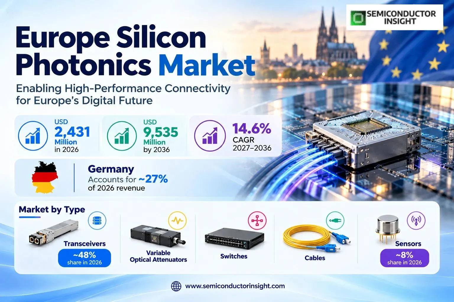
- Market valuation: the europe silicon photonics market is valued at USD 2,431 million in 2026, with a projection of USD 9,535 million in 2036 at 14.6% CAGR during 2027–2036. The product boundary concentrates on integrated photonic devices and associated silicon-photonics components and excludes revenue belonging to unrelated end equipment.
- Largest product class: Transceivers holds an estimated ~48% of 2026 sales, while Sensors is positioned for changing design requirements; PIC integration moves optical signal manipulation from discrete assemblies to repeatable semiconductor process flows. Continued qualification and sourcing decisions determine the pace at which that opportunity becomes recognized commercial revenue.
- Application demand: Data Center and Computing contributes an estimated ~38% of 2026 revenue because AI cluster optical interconnect, metro transport, photonic sensing and research-to-volume manufacturing. Suppliers must translate end-user needs into components tested for the host system, rather than count entire equipment budgets as optical-product sales.
- Geographic concentration: Germany represents an estimated ~27% of 2026 market turnover. Demand is influenced by European chip pilot lines and local infrastructure investment; the other geographic blocks are distinct purchasing environments and are not assumed to share the same product mix or buying cycle.
- Principal constraint: External laser integration, optical alignment, thermal limits and wafer-level testing remain the major limitations on conversion from technical interest to deployments. Price pressure and the ability to maintain a replacement supply can outweigh first-mover product specifications in long-life infrastructure programmes.
Europe Silicon Photonics Market Overview
Europe silicon photonics market reached USD 2,431 million in 2026 and is projected at USD 9,535 million by 2036, representing a CAGR of 14.6% over the 2027–2036 forecast period. Germany accounts for an estimated ~27% of 2026 revenue, with the outlook shaped by AI cluster optical interconnect, metro transport, photonic sensing and research-to-volume manufacturing.
Europe Silicon Photonics brings together silicon waveguides, modulators, photodetectors, optical packaging and photonic integrated circuits. The saleable boundary covers integrated photonic devices and associated silicon-photonics components, which are bought through a specialized supply chain and tested to the requirements of their downstream electronic or optical equipment. Within europe silicon photonics, the market definition decision is affected by external laser integration, optical alignment, thermal limits and wafer-level testing. This scope avoids allocating the whole of a network system or finished vehicle to its optical chip or medium.
Product inclusions follow the published type classes: Transceivers, Variable Optical Attenuators, Switches, Cables, Sensors. Application demand is separated into Data Center and Computing, Telecommunication, Military, Defense & Aerospace, Medical and Life Science, Others. Closely related services, installed end devices and adjacent technologies may influence sales but are not added automatically to the semiconductor, module or media product line. Within europe silicon photonics, the revenue boundary decision is affected by external laser integration, optical alignment, thermal limits and wafer-level testing. The distinction also preserves comparability between replacement purchasing and first-time deployment.
The technical architecture depends on silicon waveguides, modulators, photodetectors, optical packaging and photonic integrated circuits. Packaging, active electrical interfaces, product lifetime and service documentation each affect the final cost more than raw functional capability. The risk increases when a promising development cannot be characterized consistently across temperatures, factories and customer qualification fixtures. Within europe silicon photonics, the technology architecture decision is affected by external laser integration, optical alignment, thermal limits and wafer-level testing. Suppliers with test capacity and known process windows are better positioned than prototype-only entrants.
Buying decisions originate in AI cluster optical interconnect, metro transport, photonic sensing and research-to-volume manufacturing. Customer procurement therefore tends to be shaped by system design windows, engineering sign-off, approved part lists and the underlying business case for replacing existing equipment. A relevant source for the technology ecosystem is STMicroelectronics and its documented programme, pic100 enters 300 mm volume production. Within europe silicon photonics, the procurement mechanism decision is affected by external laser integration, optical alignment, thermal limits and wafer-level testing. Customer projects and supplier shipments are different stages and should not be mistaken for the same volume.
The major transition for europe silicon photonics is that PIC integration moves optical signal manipulation from discrete assemblies to repeatable semiconductor process flows. This does not mean all legacy architectures disappear immediately. Procurement must still absorb external laser integration, optical alignment, thermal limits and wafer-level testing, and design qualification typically creates an offset between a technical announcement and a recurring shipment cycle. Within europe silicon photonics, the current market change decision is affected by external laser integration, optical alignment, thermal limits and wafer-level testing. The highest-value opportunities belong to repeatable designs and multi-year production programmes.
Segment Analysis: By Type
The type structure follows Transceivers, Variable Optical Attenuators, Switches, Cables, Sensors. Transceivers leads in 2026 at an estimated ~48% share, while Sensors represents ~8% with an indicative ~19.5% growth profile. Product functionality alone is insufficient to establish a sale; compatible interfaces and qualified manufacturing decide the design slot. Within europe silicon photonics, the product segmentation decision is affected by external laser integration, optical alignment, thermal limits and wafer-level testing.
| Type | Function | Market position |
|---|---|---|
| Transceivers | Transceivers is a defined product class within europe silicon photonics, addressing an identifiable technical or deployment requirement. Its usefulness depends on host interfaces, environmental tolerance, acceptable integration cost and the ability to maintain supply beyond a single prototype. Transceivers must be specified by the buyer before a product can be tested against alternatives. Within europe silicon photonics, the type transceivers decision is affected by external laser integration, optical alignment, thermal limits and wafer-level testing. foundry qualification, optical-module partnerships and chip packaging agreements conditions the opportunity. | Estimated ~48% of 2026 product revenue; ~14.1% CAGR. For Transceivers, commercial ranking reflects not only volume but also price and component complexity. This class faces a distinct adoption balance between current customer programmes and competing formats; the revenue opportunity is bounded by integrated photonic devices and associated silicon-photonics components. Within europe silicon photonics, the market position transceivers decision is affected by external laser integration, optical alignment, thermal limits and wafer-level testing. Customers will not necessarily replace existing qualified hardware when a newer design becomes available. |
| Variable Optical Attenuators | Variable Optical Attenuators is a defined product class within europe silicon photonics, addressing an identifiable technical or deployment requirement. In Variable Optical Attenuators products, its usefulness depends on host interfaces, environmental tolerance, acceptable integration cost and the ability to maintain supply beyond a single prototype. Variable Optical Attenuators must be specified by the buyer before a product can be tested against alternatives. Within europe silicon photonics, the type variable optical attenuators decision is affected by external laser integration, optical alignment, thermal limits and wafer-level testing. foundry qualification, optical-module partnerships and chip packaging agreements conditions the opportunity. | Estimated ~17% of 2026 product revenue; ~14.1% CAGR. For Variable Optical Attenuators, commercial ranking reflects not only volume but also price and component complexity. In Variable Optical Attenuators procurement, this class faces a distinct adoption balance between current customer programmes and competing formats; the revenue opportunity is bounded by integrated photonic devices and associated silicon-photonics components. Within europe silicon photonics, the market position variable optical attenuators decision is affected by external laser integration, optical alignment, thermal limits and wafer-level testing. In Variable Optical Attenuators procurement, customers will not necessarily replace existing qualified hardware when a newer design becomes available. |
| Switches | Switches is a defined product class within europe silicon photonics, addressing an identifiable technical or deployment requirement. In Switches products, its usefulness depends on host interfaces, environmental tolerance, acceptable integration cost and the ability to maintain supply beyond a single prototype. Switches must be specified by the buyer before a product can be tested against alternatives. Within europe silicon photonics, the type switches decision is affected by external laser integration, optical alignment, thermal limits and wafer-level testing. foundry qualification, optical-module partnerships and chip packaging agreements conditions the opportunity. | Estimated ~16% of 2026 product revenue; ~14.1% CAGR. For Switches, commercial ranking reflects not only volume but also price and component complexity. In Switches procurement, this class faces a distinct adoption balance between current customer programmes and competing formats; the revenue opportunity is bounded by integrated photonic devices and associated silicon-photonics components. Within europe silicon photonics, the market position switches decision is affected by external laser integration, optical alignment, thermal limits and wafer-level testing. In Switches procurement, customers will not necessarily replace existing qualified hardware when a newer design becomes available. |
| Cables | Cables is a defined product class within europe silicon photonics, addressing an identifiable technical or deployment requirement. In Cables products, its usefulness depends on host interfaces, environmental tolerance, acceptable integration cost and the ability to maintain supply beyond a single prototype. Cables must be specified by the buyer before a product can be tested against alternatives. Within europe silicon photonics, the type cables decision is affected by external laser integration, optical alignment, thermal limits and wafer-level testing. foundry qualification, optical-module partnerships and chip packaging agreements conditions the opportunity. | Estimated ~11% of 2026 product revenue; ~14.1% CAGR. For Cables, commercial ranking reflects not only volume but also price and component complexity. In Cables procurement, this class faces a distinct adoption balance between current customer programmes and competing formats; the revenue opportunity is bounded by integrated photonic devices and associated silicon-photonics components. Within europe silicon photonics, the market position cables decision is affected by external laser integration, optical alignment, thermal limits and wafer-level testing. In Cables procurement, customers will not necessarily replace existing qualified hardware when a newer design becomes available. |
| Sensors | Sensors is a defined product class within europe silicon photonics, addressing an identifiable technical or deployment requirement. In Sensors products, its usefulness depends on host interfaces, environmental tolerance, acceptable integration cost and the ability to maintain supply beyond a single prototype. Sensors must be specified by the buyer before a product can be tested against alternatives. Within europe silicon photonics, the type sensors decision is affected by external laser integration, optical alignment, thermal limits and wafer-level testing. foundry qualification, optical-module partnerships and chip packaging agreements conditions the opportunity. | Estimated ~8% of 2026 product revenue; ~19.5% CAGR. For Sensors, commercial ranking reflects not only volume but also price and component complexity. In Sensors procurement, this class faces a distinct adoption balance between current customer programmes and competing formats; the revenue opportunity is bounded by integrated photonic devices and associated silicon-photonics components. Within europe silicon photonics, the market position sensors decision is affected by external laser integration, optical alignment, thermal limits and wafer-level testing. In Sensors procurement, customers will not necessarily replace existing qualified hardware when a newer design becomes available. |
Secondary segmentation: commercial and integration axes
A commercial segmentation can be useful alongside the source-defined type breakdown, particularly when determining the distinction between a packaged module, a technology platform and an integrated final system. These illustrative purchasing stages do not alter the published product classes. Within europe silicon photonics, the commercial structure decision is affected by external laser integration, optical alignment, thermal limits and wafer-level testing.
| Axis | Members | Commercial role |
|---|---|---|
| By Integration | Chip integration · Packaged module · System qualification | By Integration in europe silicon photonics separates the design responsibility among Chip integration, Packaged module, System qualification. For By Integration in europe silicon photonics, these commercial routes influence who owns final reliability testing, firmware validation, component interchangeability and qualification documentation. Buyers in the europe silicon photonics market selecting Chip integration often have different engineering resources from integrators sourcing pre-tested modules. Within europe silicon photonics, the By Integration commercial segmentation decision is affected by external laser integration, optical alignment, thermal limits and wafer-level testing. |
| By Channel | Direct supply agreement · OEM-integrated component · Distributor-qualified part | By Channel in europe silicon photonics separates the design responsibility among Direct supply agreement, OEM-integrated component, Distributor-qualified part. For By Channel in europe silicon photonics, these commercial routes influence who owns final reliability testing, firmware validation, component interchangeability and qualification documentation. Buyers in the europe silicon photonics market selecting Direct supply agreement often have different engineering resources from integrators sourcing pre-tested modules. Within europe silicon photonics, the By Channel commercial segmentation decision is affected by external laser integration, optical alignment, thermal limits and wafer-level testing. |
Segment Analysis: By Application
Applications in the market comprise Data Center and Computing, Telecommunication, Military, Defense & Aerospace, Medical and Life Science, Others. Data Center and Computing leads at an estimated ~38% of 2026 value. Each application has different performance thresholds, testing obligations, replacement cycles and commercial access, which means total installations cannot be treated as direct sales of the narrower product. Within europe silicon photonics, the applications decision is affected by external laser integration, optical alignment, thermal limits and wafer-level testing.
| Application | Demand characteristics |
|---|---|
| Data Center and Computing | An estimated ~38% share of 2026 revenue; ~16.0% CAGR. Data Center and Computing buyers prioritize the function of silicon waveguides, modulators, photodetectors, optical packaging and photonic integrated circuits under their own reliability, access and procurement conditions. Engineering approval must precede larger purchase orders, and the purchasing process can operate through specialized suppliers rather than direct orders from end customers. Within europe silicon photonics, the application data center and computing decision is affected by external laser integration, optical alignment, thermal limits and wafer-level testing. Compared with adjacent deployments, the practical value is defined by accepted test results and product supply terms. |
| Telecommunication | An estimated ~31% share of 2026 revenue; ~13.6% CAGR. Telecommunication buyers prioritize the function of silicon waveguides, modulators, photodetectors, optical packaging and photonic integrated circuits under their own reliability, access and procurement conditions. In Telecommunication applications, engineering approval must precede larger purchase orders, and the purchasing process can operate through specialized suppliers rather than direct orders from end customers. Within europe silicon photonics, the application telecommunication decision is affected by external laser integration, optical alignment, thermal limits and wafer-level testing. In Telecommunication applications, compared with adjacent deployments, the practical value is defined by accepted test results and product supply terms. |
| Military, Defense & Aerospace | An estimated ~12% share of 2026 revenue; ~13.4% CAGR. Military, Defense & Aerospace buyers prioritize the function of silicon waveguides, modulators, photodetectors, optical packaging and photonic integrated circuits under their own reliability, access and procurement conditions. In Military, Defense & Aerospace applications, engineering approval must precede larger purchase orders, and the purchasing process can operate through specialized suppliers rather than direct orders from end customers. Within europe silicon photonics, the application military, defense & aerospace decision is affected by external laser integration, optical alignment, thermal limits and wafer-level testing. In Military, Defense & Aerospace applications, compared with adjacent deployments, the practical value is defined by accepted test results and product supply terms. |
| Medical and Life Science | An estimated ~10% share of 2026 revenue; ~15.4% CAGR. Medical and Life Science buyers prioritize the function of silicon waveguides, modulators, photodetectors, optical packaging and photonic integrated circuits under their own reliability, access and procurement conditions. In Medical and Life Science applications, engineering approval must precede larger purchase orders, and the purchasing process can operate through specialized suppliers rather than direct orders from end customers. Within europe silicon photonics, the application medical and life science decision is affected by external laser integration, optical alignment, thermal limits and wafer-level testing. In Medical and Life Science applications, compared with adjacent deployments, the practical value is defined by accepted test results and product supply terms. |
| Others | An estimated ~9% share of 2026 revenue; ~12.7% CAGR. Others buyers prioritize the function of silicon waveguides, modulators, photodetectors, optical packaging and photonic integrated circuits under their own reliability, access and procurement conditions. In Others applications, engineering approval must precede larger purchase orders, and the purchasing process can operate through specialized suppliers rather than direct orders from end customers. Within europe silicon photonics, the application others decision is affected by external laser integration, optical alignment, thermal limits and wafer-level testing. In Others applications, compared with adjacent deployments, the practical value is defined by accepted test results and product supply terms. |
The sales channel for the application segmentation is foundry qualification, optical-module partnerships and chip packaging agreements. An application opportunity can involve several equipment makers, but only the applicable component, module or disc shipment belongs within the product market. Service contracts and unrelated hardware should not be double-counted. Within europe silicon photonics, the application channel decision is affected by external laser integration, optical alignment, thermal limits and wafer-level testing. Demand also depends on buyer budgets and how rapidly existing equipment reaches replacement age.
Regional Analysis
Regional demand is led by Germany (~27%), France (~23%), Netherlands & Belgium (~21%) on an estimated 2026 revenue basis. Germany shows the strongest modeled expansion at ~16.1% CAGR. The geographic demand pattern is shaped by European chip pilot lines and local infrastructure investment, with customer qualification requirements and import exposure differing significantly across locations. Within europe silicon photonics, the regional analysis decision is affected by external laser integration, optical alignment, thermal limits and wafer-level testing.
Why do markets for europe silicon photonics develop at different rates?
Each region buys integrated photonic devices and associated silicon-photonics components through distinct industrial structures. High-value deployments may be concentrated near major engineering centers while routine purchases can be arranged through distributors and integrated equipment vendors. External laser integration, optical alignment, thermal limits and wafer-level testing are not equally burdensome across all customer groups. Within europe silicon photonics, the regional comparisons decision is affected by external laser integration, optical alignment, thermal limits and wafer-level testing. Supplier coverage depends on available technical support and a credible service plan.
| Region | Position | Growth outlook | Demand profile | What decides supplier selection |
|---|---|---|---|---|
| Germany | Largest (~27%) | ~16.1% CAGR | industrial networks | Qualification, 2026–2036 |
| France | Established (~23%) | ~13.7% CAGR | 300 networks | Qualification, 2026–2036 |
| United Kingdom | Specialized (~17%) | ~13.5% CAGR | research-intensive networks | Qualification, 2026–2036 |
| Netherlands & Belgium | Emerging (~21%) | ~15.5% CAGR | photonic networks | Qualification, 2026–2036 |
| Southern Europe | Developing (~12%) | ~12.8% CAGR | PIC networks | Qualification, 2026–2036 |
Competitive Landscape
Competition in the europe silicon photonics market takes place across product manufacturers, component designers, integrators and research infrastructure rather than a single undifferentiated list. The published profile set covers STMicroelectronics, IMEC, ams AG, II-VI Incorporated, Seagate Technology and others. The commercial distinction matters because company-wide revenue does not identify revenue from integrated photonic devices and associated silicon-photonics components. Within europe silicon photonics, the competitive landscape decision is affected by external laser integration, optical alignment, thermal limits and wafer-level testing.
Commercial differentiation begins with silicon waveguides, modulators, photodetectors, optical packaging and photonic integrated circuits; qualification quality and production yield usually decide recurring orders. Within europe silicon photonics, the competition 0 decision is affected by external laser integration, optical alignment, thermal limits and wafer-level testing. Product acceptance in this competition 0 context hinges on traceable specifications, qualification responsibility, approved sourcing and the operating lifetime expected by buyers.
Supplier strategies reflect foundry qualification, optical-module partnerships and chip packaging agreements, including the differences between catalog components and custom customer-designed products. Within europe silicon photonics, the competition 1 decision is affected by external laser integration, optical alignment, thermal limits and wafer-level testing. Product acceptance in this competition 1 context hinges on traceable specifications, qualification responsibility, approved sourcing and the operating lifetime expected by buyers.
Competition intensifies when customers can substitute equivalent components without changing the host design. External laser integration, optical alignment, thermal limits and wafer-level testing can preserve an incumbent advantage when approved designs are expensive to requalify. Within europe silicon photonics, the competition 2 decision is affected by external laser integration, optical alignment, thermal limits and wafer-level testing.
The full player landscape includes Luxtera (acquired by Cisco), LioniX International, Effect Photonics, VLC Photonics (now part of Hitachi High-Tech). Some names represent legacy subsidiaries, institutional partners or finished-system companies rather than direct shipments of the defined optical product. Within europe silicon photonics, the competition 3 decision is affected by external laser integration, optical alignment, thermal limits and wafer-level testing.
Tier structure
| Tier | Companies | Basis of competition |
|---|---|---|
| Tier 1 | STMicroelectronics; Effect Photonics | This tier groups participants by their direct exposure to integrated photonic devices and associated silicon-photonics components and by whether they manufacture, integrate or enable the technology. Supplier qualification, delivery continuity, customer support and ownership of proprietary design form the important differentiators. The companies shown in this tier may operate different business models. Within europe silicon photonics, the tier 0 decision is affected by external laser integration, optical alignment, thermal limits and wafer-level testing. System and platform partners are separated where a sale of the final machine does not imply chip or module manufacturing. |
| Tier 2 | LioniX International; ams AG; related photonics manufacturers | In Tier 2 suppliers, this tier groups participants by their direct exposure to integrated photonic devices and associated silicon-photonics components and by whether they manufacture, integrate or enable the technology. In Tier 2 suppliers, supplier qualification, delivery continuity, customer support and ownership of proprietary design form the important differentiators. The companies shown in this tier may operate different business models. Within europe silicon photonics, the tier 1 decision is affected by external laser integration, optical alignment, thermal limits and wafer-level testing. In Tier 2 suppliers, system and platform partners are separated where a sale of the final machine does not imply chip or module manufacturing. |
| Tier 3 | IMEC; Rockley Photonics; Luxtera (Cisco); Seagate Technology; II-VI; VLC Photonics (Hitachi High-Tech) | In Tier 3 suppliers, this tier groups participants by their direct exposure to integrated photonic devices and associated silicon-photonics components and by whether they manufacture, integrate or enable the technology. In Tier 3 suppliers, supplier qualification, delivery continuity, customer support and ownership of proprietary design form the important differentiators. The companies shown in this tier may operate different business models. Within europe silicon photonics, the tier 2 decision is affected by external laser integration, optical alignment, thermal limits and wafer-level testing. In Tier 3 suppliers, system and platform partners are separated where a sale of the final machine does not imply chip or module manufacturing. |
Key companies profiled
- STMicroelectronics
- IMEC
- ams AG
- II-VI Incorporated
- Seagate Technology
- Rockley Photonics
- Luxtera (acquired by Cisco)
- LioniX International
- Effect Photonics
- VLC Photonics (now part of Hitachi High-Tech)
Production Capacity Analysis
Production capability for europe silicon photonics depends on silicon waveguides, modulators, photodetectors, optical packaging and photonic integrated circuits and on specialized testing, packaging and reliable material supply. Technical capacity must be distinguished from publicly announced facility investment and from customer shipments. Access to product-specific process controls is a leading determinant of scalable output. Within europe silicon photonics, the production decision is affected by external laser integration, optical alignment, thermal limits and wafer-level testing.
Upstream manufacturing capacity is constrained by external laser integration, optical alignment, thermal limits and wafer-level testing. Even where wafer fabrication, media coating or optical-module lines are available, the practical yield of acceptable finished products depends on optical testing, error screening and customer-specific reliability sign-off. Within europe silicon photonics, the production economics decision is affected by external laser integration, optical alignment, thermal limits and wafer-level testing.
Alternative sourcing and regional capacity matter when foundry qualification, optical-module partnerships and chip packaging agreements. Cross-border suppliers need compatible technical documentation and reliable logistics, whereas customers with long-life products may pay more for second-source approval and stable manufacturing change control. Within europe silicon photonics, the production geography decision is affected by external laser integration, optical alignment, thermal limits and wafer-level testing.
Upstream inputs include specialist materials, optoelectronic assemblies, precision equipment and software for verification of integrated photonic devices and associated silicon-photonics components. A supplier can have nominal capacity without enough verified test throughput, making test fixtures, skilled process engineering and reliable device packaging important practical bottlenecks. Within europe silicon photonics, the production constraints decision is affected by external laser integration, optical alignment, thermal limits and wafer-level testing.
Market Dynamics
Growth and adoption reflect several interacting drivers: AI cluster optical interconnect, metro transport, photonic sensing and research-to-volume manufacturing, shifts in integration efficiency and procurement decisions. Countervailing factors include external laser integration, optical alignment, thermal limits and wafer-level testing. Consequently, market growth does not translate mechanically into identical growth for every product, customer application or country. Within europe silicon photonics, the market dynamics decision is affected by external laser integration, optical alignment, thermal limits and wafer-level testing.
MARKET DRIVERS
Drivers Impact Analysis*
| Driver | (~) % impact on CAGR forecast | Geographic relevance | Impact timeline |
|---|---|---|---|
| Growth in end-user technical requirements | +2.3% | Europe | 2026–2036 |
| New integration and manufacturing platforms | +1.7% | Europe | 2027–2036 |
| Customer qualification and design wins | +1.2% | Europe | 2028–2036 |
| Changes in data, mobility and infrastructure | +0.8% | Europe | 2029–2036 |
| Regional industrial investment | +0.6% | Europe | 2030–2036 |
Growth in end-user technical requirements
Growth in end-user technical requirements matters because PIC integration moves optical signal manipulation from discrete assemblies to repeatable semiconductor process flows. The uptake depends on tangible demand for AI cluster optical interconnect, metro transport, photonic sensing and research-to-volume manufacturing, followed by the successful integration of components within a complete customer system. Within europe silicon photonics, the driver growth in end-user technical requirements decision is affected by external laser integration, optical alignment, thermal limits and wafer-level testing. Near-term engineering awards must be separated from repeat production revenue.
New integration and manufacturing platforms
New integration and manufacturing platforms matters because PIC integration moves optical signal manipulation from discrete assemblies to repeatable semiconductor process flows. In new integration and manufacturing platforms factor, the uptake depends on tangible demand for AI cluster optical interconnect, metro transport, photonic sensing and research-to-volume manufacturing, followed by the successful integration of components within a complete customer system. Within europe silicon photonics, the driver new integration and manufacturing platforms decision is affected by external laser integration, optical alignment, thermal limits and wafer-level testing. Near-term engineering awards must be separated from repeat production revenue.
Customer qualification and design wins
Customer qualification and design wins matters because PIC integration moves optical signal manipulation from discrete assemblies to repeatable semiconductor process flows. In customer qualification and design wins factor, the uptake depends on tangible demand for AI cluster optical interconnect, metro transport, photonic sensing and research-to-volume manufacturing, followed by the successful integration of components within a complete customer system. Within europe silicon photonics, the driver customer qualification and design wins decision is affected by external laser integration, optical alignment, thermal limits and wafer-level testing. Near-term engineering awards must be separated from repeat production revenue.
Changes in data, mobility and infrastructure
Changes in data, mobility and infrastructure matters because PIC integration moves optical signal manipulation from discrete assemblies to repeatable semiconductor process flows. In changes in data, mobility and infrastructure factor, the uptake depends on tangible demand for AI cluster optical interconnect, metro transport, photonic sensing and research-to-volume manufacturing, followed by the successful integration of components within a complete customer system. Within europe silicon photonics, the driver changes in data, mobility and infrastructure decision is affected by external laser integration, optical alignment, thermal limits and wafer-level testing. Near-term engineering awards must be separated from repeat production revenue.
MARKET RESTRAINTS
Restraints Impact Analysis*
| Restraint | (~) % impact on CAGR forecast | Geographic relevance | Impact timeline |
|---|---|---|---|
| Upfront engineering and validation cost | −1.1% | Europe | 2026–2035 |
| Fragmented compatibility and interfaces | −0.9% | Europe | 2027–2035 |
| Price competition from adjacent technology | −0.7% | Europe | 2028–2035 |
| Concentration of critical manufacturing capacity | −0.5% | Europe | 2029–2035 |
Upfront engineering and validation cost
Upfront engineering and validation cost is a binding issue wherever external laser integration, optical alignment, thermal limits and wafer-level testing. Suppliers face pressure to validate the functional specification at scale and provide stable lifecycle support. When alternatives are already qualified and supported, buyer migration can be slower than raw market demand indicators suggest. Within europe silicon photonics, the restraint upfront engineering and validation cost decision is affected by external laser integration, optical alignment, thermal limits and wafer-level testing. Complex qualification is especially material for long-lived infrastructure and compliance-sensitive purchases.
Fragmented compatibility and interfaces
Fragmented compatibility and interfaces is a binding issue wherever external laser integration, optical alignment, thermal limits and wafer-level testing. In fragmented compatibility and interfaces factor, suppliers face pressure to validate the functional specification at scale and provide stable lifecycle support. In fragmented compatibility and interfaces factor, when alternatives are already qualified and supported, buyer migration can be slower than raw market demand indicators suggest. Within europe silicon photonics, the restraint fragmented compatibility and interfaces decision is affected by external laser integration, optical alignment, thermal limits and wafer-level testing. Complex qualification is especially material for long-lived infrastructure and compliance-sensitive purchases.
Price competition from adjacent technology
Price competition from adjacent technology is a binding issue wherever external laser integration, optical alignment, thermal limits and wafer-level testing. In price competition from adjacent technology factor, suppliers face pressure to validate the functional specification at scale and provide stable lifecycle support. In price competition from adjacent technology factor, when alternatives are already qualified and supported, buyer migration can be slower than raw market demand indicators suggest. Within europe silicon photonics, the restraint price competition from adjacent technology decision is affected by external laser integration, optical alignment, thermal limits and wafer-level testing. Complex qualification is especially material for long-lived infrastructure and compliance-sensitive purchases.
Concentration of critical manufacturing capacity
Concentration of critical manufacturing capacity is a binding issue wherever external laser integration, optical alignment, thermal limits and wafer-level testing. In concentration of critical manufacturing capacity factor, suppliers face pressure to validate the functional specification at scale and provide stable lifecycle support. In concentration of critical manufacturing capacity factor, when alternatives are already qualified and supported, buyer migration can be slower than raw market demand indicators suggest. Within europe silicon photonics, the restraint concentration of critical manufacturing capacity decision is affected by external laser integration, optical alignment, thermal limits and wafer-level testing. Complex qualification is especially material for long-lived infrastructure and compliance-sensitive purchases.
MARKET OPPORTUNITIES
Customer upgrades and installation renewal
Customer upgrades and installation renewal creates space for suppliers able to deliver integrated photonic devices and associated silicon-photonics components against verified acceptance criteria. The advantage may come from better integration, predictable production, or more dependable support rather than nominal top-line performance. Within europe silicon photonics, the opportunity customer upgrades and installation renewal decision is affected by external laser integration, optical alignment, thermal limits and wafer-level testing. Foundry qualification, optical-module partnerships and chip packaging agreements must translate interest into purchase orders.
More integrated product architectures
More integrated product architectures creates space for suppliers able to deliver integrated photonic devices and associated silicon-photonics components against verified acceptance criteria. In more integrated product architectures factor, the advantage may come from better integration, predictable production, or more dependable support rather than nominal top-line performance. Within europe silicon photonics, the opportunity more integrated product architectures decision is affected by external laser integration, optical alignment, thermal limits and wafer-level testing. In more integrated product architectures factor, foundry qualification, optical-module partnerships and chip packaging agreements must translate interest into purchase orders.
Expansion through industrial partnerships
Expansion through industrial partnerships creates space for suppliers able to deliver integrated photonic devices and associated silicon-photonics components against verified acceptance criteria. In expansion through industrial partnerships factor, the advantage may come from better integration, predictable production, or more dependable support rather than nominal top-line performance. Within europe silicon photonics, the opportunity expansion through industrial partnerships decision is affected by external laser integration, optical alignment, thermal limits and wafer-level testing. In expansion through industrial partnerships factor, foundry qualification, optical-module partnerships and chip packaging agreements must translate interest into purchase orders.
Reliability-focused specialized deployments
Reliability-focused specialized deployments creates space for suppliers able to deliver integrated photonic devices and associated silicon-photonics components against verified acceptance criteria. In reliability-focused specialized deployments factor, the advantage may come from better integration, predictable production, or more dependable support rather than nominal top-line performance. Within europe silicon photonics, the opportunity reliability-focused specialized deployments decision is affected by external laser integration, optical alignment, thermal limits and wafer-level testing. In reliability-focused specialized deployments factor, foundry qualification, optical-module partnerships and chip packaging agreements must translate interest into purchase orders.
Supply Chain Analysis
The europe silicon photonics supply chain links specialized upstream materials and design intellectual property to process engineering, product testing, qualified integration and end-use customers. The importance of each link depends on silicon waveguides, modulators, photodetectors, optical packaging and photonic integrated circuits. Contractual control of the production and qualification process matters as much as control of the initial design. Within europe silicon photonics, the supply chain decision is affected by external laser integration, optical alignment, thermal limits and wafer-level testing.
Upstream. Upstream activities determine the product cost, acceptance criteria and delivery commitments associated with integrated photonic devices and associated silicon-photonics components. In practice, specifications evolve through supplier-customer collaboration, and a failure at one stage may delay adoption even when the core optical technology is technically strong. Within europe silicon photonics, the supply upstream decision is affected by external laser integration, optical alignment, thermal limits and wafer-level testing. External laser integration, optical alignment, thermal limits and wafer-level testing can shape contract terms and warranty responsibilities.
Manufacturing. Manufacturing activities determine the product cost, acceptance criteria and delivery commitments associated with integrated photonic devices and associated silicon-photonics components. In manufacturing participants, in practice, specifications evolve through supplier-customer collaboration, and a failure at one stage may delay adoption even when the core optical technology is technically strong. Within europe silicon photonics, the supply manufacturing decision is affected by external laser integration, optical alignment, thermal limits and wafer-level testing. In manufacturing participants, external laser integration, optical alignment, thermal limits and wafer-level testing can shape contract terms and warranty responsibilities.
Channel. Channel activities determine the product cost, acceptance criteria and delivery commitments associated with integrated photonic devices and associated silicon-photonics components. In channel participants, in practice, specifications evolve through supplier-customer collaboration, and a failure at one stage may delay adoption even when the core optical technology is technically strong. Within europe silicon photonics, the supply channel decision is affected by external laser integration, optical alignment, thermal limits and wafer-level testing. In channel participants, external laser integration, optical alignment, thermal limits and wafer-level testing can shape contract terms and warranty responsibilities.
Downstream. Downstream activities determine the product cost, acceptance criteria and delivery commitments associated with integrated photonic devices and associated silicon-photonics components. In downstream participants, in practice, specifications evolve through supplier-customer collaboration, and a failure at one stage may delay adoption even when the core optical technology is technically strong. Within europe silicon photonics, the supply downstream decision is affected by external laser integration, optical alignment, thermal limits and wafer-level testing. In downstream participants, external laser integration, optical alignment, thermal limits and wafer-level testing can shape contract terms and warranty responsibilities.
Recent Developments
- 21 May 2026 Published
PIXEurope Connect industry event. PIXEurope Connect brought industry and public institutions together in Barcelona to advance European PIC pilot-line access. The documented action affects europe silicon photonics because PIC integration moves optical signal manipulation from discrete assemblies to repeatable semiconductor process flows. The implementation path still requires supplier-specific qualification and a clear distinction between development activity, related system deployment and recurring sales of integrated photonic devices and associated silicon-photonics components. Buyers will assess the effect on performance, supply assurance and maintenance rather than treating a single corporate announcement as immediate market revenue. Source - 9 Mar 2026 Published
PIC100 enters 300 mm volume production. ST began high-volume PIC100 production on 300 mm wafers and described plans to multiply capacity by 2027. In 9 Mar 2026 100 enters 300 mm volume production, the documented action affects europe silicon photonics because PIC integration moves optical signal manipulation from discrete assemblies to repeatable semiconductor process flows. In 9 Mar 2026 100 enters 300 mm volume production, the implementation path still requires supplier-specific qualification and a clear distinction between development activity, related system deployment and recurring sales of integrated photonic devices and associated silicon-photonics components. In 9 Mar 2026 100 enters 300 mm volume production, buyers will assess the effect on performance, supply assurance and maintenance rather than treating a single corporate announcement as immediate market revenue. Source - 23 Sep 2025 Published
STARLight 300 mm SiPho consortium. ST announced the STARLight consortium spanning 24 organizations and 11 EU countries for 300 mm silicon photonics. In 23 Sep 2025 g>STARLight 300 mm SiPho consortium, the documented action affects europe silicon photonics because PIC integration moves optical signal manipulation from discrete assemblies to repeatable semiconductor process flows. In 23 Sep 2025 g>STARLight 300 mm SiPho consortium, the implementation path still requires supplier-specific qualification and a clear distinction between development activity, related system deployment and recurring sales of integrated photonic devices and associated silicon-photonics components. In 23 Sep 2025 g>STARLight 300 mm SiPho consortium, buyers will assess the effect on performance, supply assurance and maintenance rather than treating a single corporate announcement as immediate market revenue. Source - 20 Feb 2025 Published
Silicon photonics for optical AI interconnect. ST outlined a new silicon-photonics platform and its development collaboration with Amazon Web Services. In 20 Feb 2025 otonics for optical AI interconnect, the documented action affects europe silicon photonics because PIC integration moves optical signal manipulation from discrete assemblies to repeatable semiconductor process flows. In 20 Feb 2025 otonics for optical AI interconnect, the implementation path still requires supplier-specific qualification and a clear distinction between development activity, related system deployment and recurring sales of integrated photonic devices and associated silicon-photonics components. In 20 Feb 2025 otonics for optical AI interconnect, buyers will assess the effect on performance, supply assurance and maintenance rather than treating a single corporate announcement as immediate market revenue. Source - 16 Jan 2025 Published
Five Chips for Europe pilot lines. The European Commission launched the first Chips for Europe pilot-line cohort with photonics as a named technology area. In 16 Jan 2025 g>Five Chips for Europe pilot lines, the documented action affects europe silicon photonics because PIC integration moves optical signal manipulation from discrete assemblies to repeatable semiconductor process flows. In 16 Jan 2025 g>Five Chips for Europe pilot lines, the implementation path still requires supplier-specific qualification and a clear distinction between development activity, related system deployment and recurring sales of integrated photonic devices and associated silicon-photonics components. In 16 Jan 2025 g>Five Chips for Europe pilot lines, buyers will assess the effect on performance, supply assurance and maintenance rather than treating a single corporate announcement as immediate market revenue. Source - 24 Jun 2024 Published
Photonics pilot-line support. The Commission announced financial support for a photonics pilot line and chip competence centres. In 24 Jun 2024 strong>Photonics pilot-line support, the documented action affects europe silicon photonics because PIC integration moves optical signal manipulation from discrete assemblies to repeatable semiconductor process flows. In 24 Jun 2024 strong>Photonics pilot-line support, the implementation path still requires supplier-specific qualification and a clear distinction between development activity, related system deployment and recurring sales of integrated photonic devices and associated silicon-photonics components. In 24 Jun 2024 strong>Photonics pilot-line support, buyers will assess the effect on performance, supply assurance and maintenance rather than treating a single corporate announcement as immediate market revenue. Source
REPORT SCOPE & SEGMENTATION
| Attribute | Details |
|---|---|
| Study Period | 2021–2036 |
| Base Year | 2026 |
| Estimated Year | 2027 |
| Forecast Period | 2027–2036 |
| 2026 Market Size | USD 2,431 million |
| 2027 Market Estimate | USD 2,787 million |
| 2036 Projected Market Size | USD 9,535 million |
| Growth Rate | 14.6% CAGR (2027–2036) |
| Reporting Unit | USD million |
| Product Boundary | integrated photonic devices and associated silicon-photonics components |
| By Type | Transceivers · Variable Optical Attenuators · Switches · Cables · Sensors |
| By Application | Data Center and Computing · Telecommunication · Military, Defense & Aerospace · Medical and Life Science · Others |
| By Region | Europe-only study; each comparison block represents a national or subregional market. GermanyBerlin; Dresden; Munich; Stuttgart FranceCrolles; Grenoble; Paris; Saclay United KingdomLondon; Cambridge; Southampton; Bristol Netherlands & BelgiumEindhoven; Enschede; Leuven; Ghent Southern EuropeBarcelona; Madrid; Milan; Turin |
| Key Companies Profiled | STMicroelectronics; IMEC; ams AG; II-VI Incorporated; Seagate Technology; Rockley Photonics; Luxtera (acquired by Cisco); LioniX International; Effect Photonics; VLC Photonics (now part of Hitachi High-Tech) |
| Customization Scope | Company and country detail, product qualification and supplier economics, volumes, pricing, cost structure, technical architectures and demand by year for integrated photonic devices and associated silicon-photonics components. |
Frequently Asked Questions
What is the Europe Silicon Photonics market size and outlook?
The europe silicon photonics market is estimated at USD 2,431 million in 2026 and projected to reach USD 9,535 million in 2036, equivalent to a 14.6% CAGR over 2027–2036. The defined revenue boundary covers integrated photonic devices and associated silicon-photonics components. The estimate reflects growth in AI cluster optical interconnect, metro transport, photonic sensing and research-to-volume manufacturing rather than the total value of finished equipment or associated services. Within europe silicon photonics, the faq 0 decision is affected by external laser integration, optical alignment, thermal limits and wafer-level testing.
Which product type leads the europe silicon photonics market?
Transceivers leads with an estimated ~48% share of 2026 product sales. It has a meaningful position because PIC integration moves optical signal manipulation from discrete assemblies to repeatable semiconductor process flows. That share is an estimate of product value, not a factory-capacity figure, and purchasers still apply their own reliability tests and approved-part controls before committing to recurring orders. Within europe silicon photonics, the faq 1 decision is affected by external laser integration, optical alignment, thermal limits and wafer-level testing.
Which type may gain adoption most rapidly?
Sensors is positioned for changing requirements and holds an estimated ~8% of 2026 market value. Its modeled growth of ~19.5% reflects an opportunity within the same product boundary. Technical readiness does not automatically guarantee purchasing adoption; product qualification, effective selling price and the installed base of alternatives remain important conditions. Within europe silicon photonics, the faq 2 decision is affected by external laser integration, optical alignment, thermal limits and wafer-level testing.
What is the leading application in this market?
Data Center and Computing generates an estimated ~38% of 2026 market revenue. This application depends on AI cluster optical interconnect, metro transport, photonic sensing and research-to-volume manufacturing, but it pays for the compatible optical product rather than the entire downstream machine, service or network. Its buying behaviour is shaped by engineering approval, total lifetime costs, supply continuity and replacement cycles. Within europe silicon photonics, the faq 3 decision is affected by external laser integration, optical alignment, thermal limits and wafer-level testing.
Which geography represents the largest revenue pool?
Germany is the largest geographic market, at an estimated ~27% of 2026 product revenue. The chief commercial context is European chip pilot lines and local infrastructure investment. The region is measured through sales attributable to integrated photonic devices and associated silicon-photonics components, so research funding, installed infrastructure and the market value of completed systems are not substituted for direct product revenue. Within europe silicon photonics, the faq 4 decision is affected by external laser integration, optical alignment, thermal limits and wafer-level testing.
Which market region is modeled to grow fastest?
Germany has the highest modeled regional revenue growth, at ~16.1% CAGR. The rate applies to an estimated share of the defined optical product and should not be taken as a published government statistic. Actual uptake will depend on project timing, technical approval and availability of qualified supply. Within europe silicon photonics, the faq 5 decision is affected by external laser integration, optical alignment, thermal limits and wafer-level testing.
What drives investment in europe silicon photonics?
The central demand drivers are AI cluster optical interconnect, metro transport, photonic sensing and research-to-volume manufacturing and the change in hardware design economics. Pic integration moves optical signal manipulation from discrete assemblies to repeatable semiconductor process flows. Customers seek a combination of acceptable performance, known operational lifetime and credible replacement support, which makes supplier relationships, field reliability and product integration important determinants of realized sales. Within europe silicon photonics, the faq 6 decision is affected by external laser integration, optical alignment, thermal limits and wafer-level testing.
What technical barriers constrain commercial scaling?
Commercial scaling remains limited by external laser integration, optical alignment, thermal limits and wafer-level testing. The impact is greatest in customer programmes where qualification tests are time-consuming or product replacement is difficult. Suppliers must demonstrate repeatable performance in manufacturing, not merely laboratory capability, and account for transport, environmental conditions, field maintenance and warranty responsibilities. Within europe silicon photonics, the faq 7 decision is affected by external laser integration, optical alignment, thermal limits and wafer-level testing.
How is the product typically purchased and supplied?
Purchasing operates through foundry qualification, optical-module partnerships and chip packaging agreements. Direct supplier involvement is more common for new designs, while replacement orders can move through approved channels after a part is qualified. This structure separates prototype revenue from established production and creates ongoing commercial value for manufacturers capable of stable lot-to-lot quality. Within europe silicon photonics, the faq 8 decision is affected by external laser integration, optical alignment, thermal limits and wafer-level testing.
What is covered by this europe silicon photonics report?
The study addresses the defined product market, its 2026–2036 outlook, type and application segmentation, supplier landscape, regional revenue mix, supply-chain constraints and commercialization trends. It preserves the published categories of Transceivers, Variable Optical Attenuators, Switches, Cables, Sensors and the applications Data Center and Computing, Telecommunication, Military, Defense & Aerospace, Medical and Life Science, Others. Figures relate to the product boundary rather than the entire surrounding equipment market. Within europe silicon photonics, the faq 9 decision is affected by external laser integration, optical alignment, thermal limits and wafer-level testing.
Research Sources & Evidence Base
Get Sample Report PDF for Exclusive Insights
Report Sample Includes
- Table of Contents
- List of Tables & Figures
- Charts, Research Methodology, and more...
 Download Sample Report PDF