Market Insights
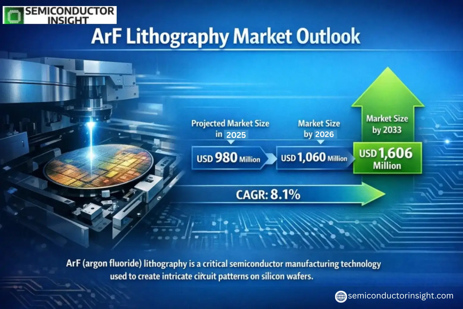
Global ArF Lithography Market size was valued at USD 980 million in 2025. The market is projected to grow from USD 1,060 million in 2026 to USD 1,606 million by 2033, exhibiting a CAGR of 8.1% during the forecast period.
ArF (argon fluoride) lithography is a critical semiconductor manufacturing technology used to create intricate circuit patterns on silicon wafers. This process utilizes deep ultraviolet (DUV) light at 193nm wavelength to enable high-resolution patterning for advanced chip fabrication. Key equipment includes ArF dry and ArFi (immersion) lithography machines, with leading models such as ASML’s TWINSCAN NXT series and Nikon’s NSR-S600 series driving innovation.
The market growth is propelled by increasing demand for smaller, more powerful semiconductor devices across consumer electronics, automotive, and AI applications. While China currently dominates with 53% market share due to aggressive semiconductor investments, the U.S. and Europe maintain significant positions with 20% and 10% shares respectively. The analog chip segment accounts for half of all applications, with integrated device manufacturers (IDMs) representing 65% of end-users. Recent technological advancements in multi-patterning techniques and improved photoresist materials are further enhancing ArF lithography’s precision capabilities.
MARKET DRIVERS
Growing Demand for Advanced Semiconductor Devices
ArF Lithography Market is driven by rising demand for high-performance chips in sectors like artificial intelligence, 5G, and IoT. Semiconductor manufacturers are adopting ArF lithography systems to produce smaller, more efficient integrated circuits with nodes below 10nm. Global semiconductor market is expected to grow at 6-8% annually, creating sustained demand for ArF lithography equipment.
Technological Advancements in Lithography Systems
Recent innovations in ArF immersion lithography have enhanced resolution capabilities, enabling production of chips with features below 38nm. Leading equipment manufacturers are developing multi-patterning techniques that extend the usability of ArF technology for advanced node production. These advancements are critical for maintaining cost-effectiveness in semiconductor manufacturing.
Manufacturers are investing in hybrid lithography solutions that combine ArF with EUV technology, ensuring continued relevance of ArF systems in next-generation semiconductor fabrication.
MARKET CHALLENGES
High Cost of Ownership and Operation
The substantial capital expenditure required for ArF lithography systems presents a significant barrier for smaller manufacturers. Maintenance costs can account for 20-25% of total ownership expenses, particularly for advanced immersion systems. The need for specialized facilities and skilled operators further increases operational challenges.
Other Challenges
Technology Transition Pressures
The semiconductor industry’s gradual shift toward EUV lithography is creating uncertainty for ArF system manufacturers. While EUV adoption is growing, the industry still relies on ArF for many critical applications, requiring careful investment balancing across lithography technologies.
MARKET RESTRAINTS
Market Saturation in Mature Nodes
As the semiconductor industry progresses beyond 10nm nodes, demand for ArF lithography in leading-edge manufacturing is facing constraints. The technology is increasingly limited to mature nodes, with EUV systems preferred for advanced applications. This is creating pricing pressures in certain segments of the ArF Lithography Market.
MARKET OPPORTUNITIES
Expansion in Emerging Semiconductor Markets
Growing semiconductor production in regions like Southeast Asia and China presents significant opportunities for ArF lithography equipment providers. These markets are investing heavily in domestic semiconductor capabilities, creating demand for both new and refurbished ArF systems. Government initiatives supporting local chip production are further driving market growth prospects.
MAIN TITLE HERE () Trends
Accelerated Market Growth Driven by Semiconductor Miniaturization
Global ArF Lithography Market, valued at USD 980 million in 2025, is projected to reach USD 1.6 billion by 2033, growing at an 8.1% CAGR. This growth is fueled by increasing demand for advanced semiconductor devices used in smartphones, IoT, and AI applications. ArF lithography systems enable the production of sub-30nm nodes, critical for next-generation chips.
Other Trends
Regional Market Concentration
China dominates the ArF Lithography Market with 53% share, followed by the U.S. (20%) and Europe (10%). Asia Pacific’s leadership stems from massive semiconductor manufacturing investments and government support for domestic chip production capabilities.
Technology Segmentation and Competitive Landscape
The market is divided between ArF dry (46% share) and ArFi immersion systems (54% share). ASML, Nikon, and SMEE collectively hold 100% market share, with ASML’s TWINSCAN NXT series and Nikon’s NSR models being industry standards. Foundries account for 35% of demand while IDMs represent 65%.
Application-Specific Growth Patterns
Analog chips represent 50% of ArF lithography applications, followed by logic chips (30%) and optical sensors (15%). The shift towards 5G and automotive semiconductors is creating new demand vectors, though supply chain constraints remain a challenge for equipment manufacturers.
Tariff Impacts and Supply Chain Dynamics
U.S. export controls and tariffs are reshaping the competitive landscape, with companies diversifying production locations. Global semiconductor shortage has accelerated capacity expansion plans, driving increased orders for ArF lithography equipment worldwide.
COMPETITIVE LANDSCAPE
Key Industry Players
Oligopolistic Market Dominance with Technological Barriers
ArF Lithography Market is dominated by ASML, Nikon, and SMEE, which collectively hold nearly 100% market share. ASML leads with its TWINSCAN NXT series, controlling approximately 70% of global capacity. The company’s technological superiority in immersion lithography and strategic partnerships with semiconductor giants like TSMC and Intel create significant entry barriers. Nikon follows with its NSR-S series, maintaining strong presence in dry ArF systems, particularly in Asian markets.
Emerging players such as Canon and Shanghai Micro Electronics Equipment (SMEE) are gradually expanding capabilities, though constrained by patent portfolios and R&D budgets. Niche participants like Ultratech and EV Group focus on specialized applications, leveraging hybrid lithography solutions. The market remains concentrated due to extreme capital intensity, with single tools costing USD 40-80 million and requiring years of field calibration.
List of Key ArF Lithography Companies Profiled
- ASML Holdings NV
- Nikon Corporation
- Shanghai Micro Electronics Equipment (SMEE)
- Canon Inc.
- Ultratech (Veeco Instruments)
- EV Group
- SUSS MicroTec
- Cymer (ASML subsidiary)
- NuFlare Technology
- Tokyo Electron Limited
- Lam Research
- Applied Materials
- KLA Corporation
- Hitachi High-Tech
- Advantest Corporation
Segment Analysis:
| Segment Category | Sub-Segments | Key Insights |
| By Type |
|
ArFi Immersion Lithography dominates due to higher resolution capabilities critical for advanced node semiconductors. Key factors:
|
| By Application |
|
Analog Chip segment leads as ArF systems are ideal for mixed-signal ICs:
|
| By End User |
|
IDM segment maintains strong market position due to:
|
| By Technology Node |
|
20-28nm node remains the sweet spot for ArF systems:
|
| By Equipment Model |
|
TWINSCAN Series maintains technology leadership through:
|
Regional Analysis: ArF Lithography Market
Taiwan accounts for over 60% of global foundry capacity, with TSMC leading ArF lithography adoption for 5nm and 3nm nodes. The concentrated semiconductor infrastructure creates efficient clustering of ArF system suppliers and service providers.
South Korean chipmakers leverage ArF lithography for advanced DRAM production, with specialized applications in high-density memory stacks. The country’s vertical integration model ensures continuous ArF technology refinement for memory applications.
Chinese semiconductor firms are developing domestic ArF lithography capabilities amid technology restrictions. Government-backed initiatives focus on achieving self-reliance in ArF systems through partnerships between research institutes and local equipment makers.
Japan maintains strong positions in ArF photoresists and ancillary materials, with chemical companies developing next-generation formulations specifically for Asia-Pacific foundries’ unique requirements.
North America
North America remains crucial for ArF lithography innovation, housing major equipment developers and leading-edge R&D facilities. The region benefits from close collaboration between semiconductor equipment manufacturers and cutting-edge research institutions. While lacking large-scale foundries, North America drives ArF technology advancements through equipment development and process innovation. The U.S. CHIPS Act has reinvigorated domestic semiconductor manufacturing, creating new demand for ArF lithography solutions in emerging fabrication clusters.
Europe
Europe maintains specialized positions in the ArF Lithography Market through ASML’s technological leadership and niche semiconductor applications. The region focuses on high-value R&D and equipment development rather than volume manufacturing. European research institutes collaborate closely with equipment makers to push ArF system capabilities, particularly for automotive and industrial applications. Recent EU semiconductor initiatives aim to strengthen the regional ecosystem connecting ArF technology developers with end-users.
Middle East & Africa
The Middle East is emerging as a potential growth area for ArF lithography, with new semiconductor investments in Abu Dhabi and Saudi Arabia focusing on specialty applications. Regional sovereign wealth funds are investing in semiconductor projects that may incorporate ArF technology. Africa shows nascent interest in semiconductor manufacturing, though current ArF lithography adoption remains limited to research institutions and small-scale pilot lines.
South America
South America’s involvement in the ArF Lithography Market remains minimal, with limited semiconductor manufacturing infrastructure. Brazil maintains small-scale analog chip production that occasionally utilizes basic ArF solutions. The region primarily serves as an end-market for chips produced elsewhere rather than a manufacturing hub for advanced semiconductor processes requiring ArF lithography.
Report Scope
This market research report provides a comprehensive analysis of the ArF Lithography Market, covering the forecast period 2025–2033. It offers detailed insights into market dynamics, technological advancements, competitive landscape, and key trends shaping the industry.
Key focus areas of the report include:
- Market Overview: The report begins with an overview outlining its current market scenario, key growth indicators, and industry transformation drivers. It discusses macroeconomic factors, demand–supply balance, regulatory landscape, and the strategic role of semiconductors in powering advancements across industries such as consumer electronics, telecommunications, and industrial automation.
- Market Size & Forecast: Historical data and future projections for revenue, unit shipments, and market value across major regions and segments.
- Segmentation Analysis: Detailed breakdown by product type, application, and end-user industry to identify high-growth segments and investment opportunities.
- Regional Insights: Insights into market performance across North America, Europe, Asia-Pacific, Latin America, and the Middle East & Africa, including country-level analysis where relevant.
- Competitive Landscape: Profiles of leading market participants, including their product offerings, R&D focus, manufacturing capacity, pricing strategies, and recent developments such as mergers, acquisitions, and partnerships.
- Technology Trends & Innovation: Assessment of emerging technologies, semiconductor design trends, fabrication techniques, and evolving industry standards.
- Market Drivers & Restraints: Evaluation of factors driving market growth along with challenges, supply chain constraints, regulatory issues, and market-entry barriers.
- Stakeholder Insights: Insights for component suppliers, OEMs, system integrators, investors, and policymakers regarding the evolving ecosystem and strategic opportunities.
Primary and secondary research methods are employed, including interviews with industry experts, data from verified sources, and real-time market intelligence to ensure the accuracy and reliability of the insights presented.
FREQUENTLY ASKED QUESTIONS:
What is the current market size of ArF Lithography Market?
-> ArF Lithography Market size was valued at USD 980 million in 2025. The market is projected to grow from USD 1,060 million in 2026 to USD 1,606 million by 2033, exhibiting a CAGR of 8.1% during the forecast period.
Which key companies operate in ArF Lithography Market?
-> Key players include ASML, Nikon, and SMEE, which collectively hold about 100% market share.
What is the expected CAGR for ArF Lithography Market?
-> The market is projected to grow at a CAGR of 8.1% during 2025-2033.
Which region dominates the ArF Lithography Market?
-> China is the largest market with a 53% share, followed by the United States (20%) and Europe (10%).
What are the major applications of ArF Lithography?
-> The largest application segment is Analog Chip (50% market share), followed by Logic Chip, Optical Sensor, and others.
Who are the primary end-users of ArF Lithography?
-> IDM (Integrated Device Manufacturers) account for about 65% of the market share, while Foundries constitute the remaining portion.

Get Sample Report PDF for Exclusive Insights
Report Sample Includes
- Table of Contents
- List of Tables & Figures
- Charts, Research Methodology, and more...