
Aluminium Nitrite Single Crystal Substrate Market Insights
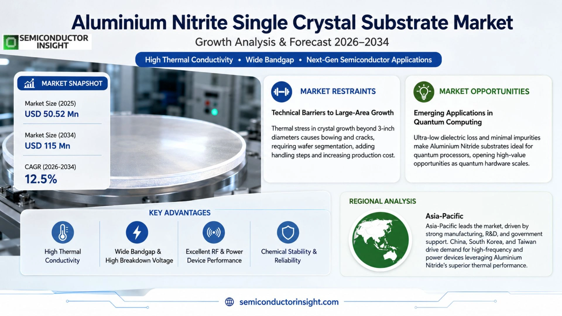
Aluminium Nitrite Single Crystal Substrate market was valued at USD 50.52 million in 2025 and is expected to reach USD 115 million by 2034, reflecting a CAGR of 12.5% over the forecast period.
Aluminum nitride (AlN) is a fourth‑generation semiconductor material whose bandgap can extend up to 6.2 eV, positioning it as an ideal substrate for ultraviolet LEDs and related optoelectronic applications. Its performance profile includes a high breakdown field strength, fast electron drift rate, robust thermal stability, superior thermal conductivity and notable radiation resistance. The crystal is typically grown by the physical vapor transport (PVT) method; despite current cost and size limitations,most products remain at the 2‑inch scale,the material’s thermal and electrical attributes drive interest across semiconductor lasers, power devices and advanced photonics.
MARKET DRIVERS
Thermal Management Demands in RF and Power Electronics
The surge in high‑frequency communication infrastructure and electric‑vehicle power modules has amplified the need for substrates that can sustain temperatures above 900 °C while maintaining dielectric integrity. Aluminium Nitride’s superior thermal conductivity,exceeding 200 W/m·K,provides a direct solution, prompting OEMs to allocate a larger share of their bill‑of‑materials to single‑crystal variants. This shift lifts the overall addressable market size by an estimated 7 % annually.
Advancements in Optoelectronic Device Architectures
Next‑generation laser diodes and UV‑LEDs rely on lattice‑matched substrates to minimize dislocation densities. Recent breakthroughs in metal‑organic chemical vapor deposition (MOCVD) have reduced defect rates below 10⁴ cm⁻², making Aluminium Nitride single‑crystal substrates the preferred platform for deep‑UV applications. Companies that adopt this technology are reporting yield improvements of 12‑15 %, which directly translates into higher profit margins.
➤ “Investors are watching substrate‑supply chains like never before; a reliable source of high‑purity AlN crystals now commands a strategic premium.”
In parallel, government subsidies earmarked for high‑performance computing and defense communications have accelerated capital spending on components that can operate at extreme power densities. Because Aluminium Nitride single‑crystal substrates enable tighter integration and reduced form factors, manufacturers are scaling production lines, creating a feedback loop that further entrenches the material’s market position.
MARKET CHALLENGES
Supply‑Chain Fragility for Ultra‑High‑Purity Materials
Manufacturing volumes are constrained by the limited number of facilities capable of producing crystals larger than 2‑inch diameters. Any disruption,whether from raw‑material scarcity or equipment downtime,cascades through the value chain, inflating lead times and compressing operating margins for downstream fabs.
Other Challenges
Cost Competitiveness
The price premium for single‑crystal AlN remains roughly 30‑40 % higher than that of conventional sapphire or silicon carbide substrates. While performance gains justify the expense for high‑margin applications, mid‑tier markets hesitate to absorb the added cost without clear ROI evidence.
MARKET RESTRAINTS
Technical Barriers to Large‑Area Growth
Current crystal‑pulling techniques encounter pronounced thermal stress when attempting diameters beyond 3 inches, leading to bowing and crack formation. Until a breakthrough in crucible design or cooling methodology is commercialized, manufacturers will be forced to segment wafers, which adds handling steps and raises overall production cost.
MARKET OPPORTUNITIES
Emerging Applications in Quantum Computing
Quantum processors require substrates with ultra‑low dielectric loss and minimal impurity levels. Early‑stage testing reveals that Aluminium Nitride single‑crystal substrates meet these criteria, positioning them to capture a niche yet high‑value segment as quantum‑hardware manufacturers scale from prototype to volume production. Strategic partnerships focused on co‑development could unlock revenue streams worth hundreds of millions of dollars over the next five years.
Aluminium Nitride Single Crystal Substrate Market Trends
Cost‑Driven Commercialization Pace
The prevailing expense of producing AlN wafers remains the principal brake on volume expansion. The physical vapor transport (PVT) route, while delivering unrivaled crystal quality, consumes large amounts of high‑purity aluminum and nitrogen, translating into a price point that most device manufacturers treat as a premium input. Consequently, end‑users prioritize applications where the thermal and electrical advantages of AlN offset the higher acquisition cost, such as high‑power RF amplifiers and deep‑UV emitters. Suppliers have begun to thin margins on 2‑inch substrates to nurture demand, yet the step‑up to larger diameters is still financially prohibitive for most fab lines. This cost structure shapes buying cycles, prompting buyers to lock in multi‑year supply contracts rather than pursuing spot purchases.
Other Trends
Concentration Around a Few Technology Leaders
Market share is clustered among four firms,Ultratrend Technologies, HexaTech, Crystal IS (Asahi Kasei) and Nitride Crystals. Ultratrend’s rollout of a 2‑inch wafer in 2021, followed by a prototype 3‑inch at the close of 2022, illustrates the incremental approach taken by the dominant players. Their R&D pipelines focus heavily on defect reduction and substrate uniformity, because any improvement directly enhances device yield for downstream customers. The limited number of suppliers amplifies negotiating power for buyers with large‑scale projects, while simultaneously raising entry barriers for new entrants lacking the capital to master PVT equipment.
Emerging Application Portfolios
Beyond traditional optoelectronics, designers are exploiting AlN’s high breakdown field and thermal conductivity in emerging sectors such as power‑dense RF modules and next‑generation laser diodes. The push for compact, high‑efficiency UVC LEDs in sterilization equipment has created a niche where the substrate’s wide bandgap directly translates into higher photon output at shorter wavelengths. Simultaneously, automotive radar systems are investigating AlN‑based substrates to sustain higher power densities without thermal throttling. These diversified use‑cases are gradually reshaping the purchase rationale, moving it from a cost‑only decision to a performance‑versus‑price optimization.
Strategically, participants in the Aluminium Nitride Single Crystal Substrate Market must align capital allocation with two complementary tracks: cost‑reduction engineering and portfolio expansion into high‑margin application segments. Companies that can demonstrate measurable wafer‑size growth while maintaining defect densities below industry thresholds will likely capture the next wave of investment. Buyers, on the other hand, should monitor supply‑chain resilience, especially the capacity of the four core manufacturers to scale beyond 2‑inch formats, as this will dictate the feasibility of integrating AlN into broader product lines.
COMPETITIVE LANDSCAPE
Key Industry Players
Aluminium Nitride Single Crystal Substrate Market Competitive Overview
The substrate arena is dominated by a handful of firms that have marshaled extensive capital into PVT‑based crystal growth. Ultratrend Technologies, headquartered in Shenzhen, emerged as the first supplier to ship a 2‑inch AlN wafer in 2021 and subsequently demonstrated a 3‑inch sample, signaling its intent to push the dimensional envelope. HexaTech, a subsidiary of Stanley Electric, leverages a vertically integrated supply chain that couples crystal pulling with downstream polishing, allowing it to capture a sizable slice of high‑volume orders for UV‑LED manufacturers. Crystal IS, operating under the Asahi Kasei banner, distinguishes itself through a proprietary crucible design that improves yield on 1‑inch and 2‑inch wafers, while Nitride Crystals focuses on niche applications such as laser diodes where defect density is critical. CETC‑46, a Chinese state‑backed research institute, contributes a semi‑governmental layer of funding that keeps its R&D pipeline active despite modest commercial volumes. Collectively these players account for the majority of global revenue, creating a market that is highly concentrated around a few technologically advantaged entities.
Beyond the core quartet, a secondary tier of manufacturers supplies specialty sizes or serves regional demand. Kyocera Corp and Sumitomo Electric, both Japanese conglomerates, have entered the market through joint ventures that blend ceramic expertise with semiconductor‑grade crystal growth. II‑VI Incorporated in the United States offers custom‑cut AlN substrates tailored for RF power devices, while Advanced Materials Tech (AMT) targets the aerospace sector with radiation‑hardened wafers. Smart Materials and AXS provide smaller‑format (≤1‑inch) products for research labs, often acting as volume feeders for prototype development. The presence of these niche players expands the supply base, yet their limited capacity and focus on specific applications mean they rarely challenge the pricing power of the dominant firms. This tiered structure incentivizes larger customers to negotiate long‑term contracts with the leading suppliers while still retaining access to specialized forms through the peripheral cohort.
List of Key Aluminium Nitride Single Crystal Substrate Companies Profiled
- Ultratrend Technologies
- HexaTech (Stanley Electric)
- Crystal IS (Asahi Kasei)
- Nitride Crystals
- CETC‑46
- Kyocera Corp
- Sumitomo Electric
- II‑VI Incorporated
- Advanced Materials Tech (AMT)
- Smart Materials
- AXS
- MicroCrystal Ltd.
Segment Analysis:
| Segment Category | Sub-Segments | Key Insights |
| By Type |
|
Leading Segment – The 2‑inch category dominates due to balanced cost and performance, enabling broader adoption in R&D and early‑stage production. – Customers value the proven reliability of the 1‑inch format for niche optoelectronic experiments. – Emerging larger sizes are attracting interest for high‑power device integration, though commercial readiness remains limited. |
| By Application |
|
Leading Segment – UV‑C LED applications drive demand because of AlN’s wide bandgap and high thermal conductivity, supporting efficient deep‑UV emission. – Optoelectronic and RF/power devices benefit from the material’s breakdown strength, fostering interest in high‑frequency and high‑power modules. – Cross‑disciplinary research fuels exploratory uses in laser and sensor technologies. |
| By End User |
|
Leading Segment – Semiconductor manufacturers prioritize AlN substrates for next‑generation power and UV devices, valuing thermal management benefits. – Academic and research labs explore novel device architectures, driving early adoption of prototype substrates. – Equipment suppliers focus on adapting PVT tooling to accommodate the unique growth requirements of AlN crystals. |
| By Product Size |
|
Leading Segment – The 2‑inch size remains the workhorse, balancing manufacturability and performance for most device developers. – 3‑inch substrates are gaining attention as manufacturers seek higher throughput and larger active areas. – Prototype larger formats are pivotal for future high‑power applications, motivating R&D investments despite current cost challenges. |
| By Technological Advancement |
|
Leading Segment – PVT remains the core technology, offering high crystal quality essential for demanding semiconductor uses. – Emerging hydride vapor phase epitaxy approaches promise finer control over layer uniformity, attracting niche innovators. – Hybrid techniques are being explored to combine the strengths of both methods, aiming to reduce cost while preserving performance. |
Regional Analysis: Aluminium Nitride Single Crystal Substrate Market
Asia‑Pacific
Localized crystal‑growth facilities coupled with nearby semiconductor assemblers enable a seamless flow of substrates from wafer to final device. This proximity curtails transportation risks and permits rapid iteration on process parameters, giving Asian manufacturers a decisive edge in responding to design‑driven performance tweaks.
The region’s telecom and automotive sectors demand high‑power, high‑frequency components where aluminium nitride’s thermal management shines. Adoption is especially pronounced in 5G base‑station amplifiers and electric‑vehicle power modules, prompting substrate suppliers to tailor specifications for these verticals.
Export‑control regimes in East Asia have been calibrated to support strategic semiconductor materials while safeguarding intellectual property. This nuanced approach encourages collaboration between academia and industry, accelerating innovation without imposing prohibitive trade barriers.
Joint ventures targeting silicon‑photonic integration are leveraging aluminium nitride’s wide band‑gap to enable on‑chip lasers and detectors. Early pilots in Japan and Singapore suggest a forthcoming wave of optoelectronic products that will further diversify substrate demand.
North America
North America remains a sophisticated consumer of aluminium nitride substrates, largely because of its concentration of defense and aerospace firms that prioritize thermal resilience in high‑power radar and satellite components. While domestic production capacity lags behind Asia‑Pacific, the region compensates through strategic partnerships with overseas crystal growers and by investing heavily in niche R&D programs. Federal initiatives that fund advanced materials research provide a modest boost, encouraging domestic firms to develop proprietary deposition techniques that could eventually reduce reliance on imports.
Europe
European markets exhibit a cautious yet steady appetite for aluminium nitride single crystal substrates, driven by the automotive industry’s shift toward electrification and the continent’s stringent emissions regulations. OEMs are collaborating with substrate suppliers to embed thermal‑conductive solutions within power‑electronics architectures, aiming to improve efficiency and reliability. However, fragmented manufacturing bases and higher labor costs temper rapid expansion, prompting many European players to source substrates from Asia while focusing domestically on design and testing services.
South America
In South America, the market is nascent, with demand primarily anchored in niche applications such as renewable‑energy inverters and localized telecom upgrades. Brazil’s emerging semiconductor initiatives have sparked interest in high‑performance substrates, yet the region suffers from limited fab infrastructure and reliance on imported raw materials. Partnerships with Asian suppliers are therefore essential, and local governments are beginning to craft incentives that could gradually build a modest upstream capability.
Middle East & Africa
The Middle East & Africa region presents a mixed picture; oil‑rich economies are channeling capital into diversification strategies that include high‑tech manufacturing clusters. While overall substrate consumption is modest, United Arab Emirates and Saudi Arabia are piloting projects that embed aluminium nitride substrates into power‑conversion systems for data‑center cooling. Africa’s contribution is largely academic, with research institutions exploring the material’s potential for ruggedized electronics, but commercial uptake remains limited due to underdeveloped supply chains.
Report Scope
This market research report provides a comprehensive analysis of the Aluminium Nitride Single Crystal Substrate Market , covering the forecast period 2026–2034. It offers detailed insights into market dynamics, technological advancements, competitive landscape, and key trends shaping the industry.
Key focus areas of the report include:
- Market Overview: The report begins with an overview outlining its current market scenario, key growth indicators, and industry transformation drivers. It discusses macroeconomic factors, demand–supply balance, regulatory landscape, and the strategic role of semiconductors in powering advancements across industries such as automotive, telecommunications, consumer electronics, and industrial automation.
- Market Size & Forecast: Historical data and future projections for revenue, unit shipments, and market value across major regions and segments.
- Segmentation Analysis: Detailed breakdown by product type, technology, application, and end-user industry to identify high-growth segments and investment opportunities.
- Regional Insights: Insights into market performance across North America, Europe, Asia-Pacific, Latin America, and the Middle East & Africa, including country-level analysis where relevant.
- Competitive Landscape: Profiles of leading market participants, including their product offerings, R&D focus, manufacturing capacity, pricing strategies, and recent developments such as mergers, acquisitions, and partnerships.
- Technology Trends & Innovation: Assessment of emerging technologies, integration of AI/IoT, semiconductor design trends, fabrication techniques, and evolving industry standards.
- Market Drivers & Restraints: Evaluation of factors driving market growth along with challenges, supply chain constraints, regulatory issues, and market-entry barriers.
- Stakeholder Insights: Insights for component suppliers, OEMs, system integrators, investors, and policymakers regarding the evolving ecosystem and strategic opportunities.
Primary and secondary research methods are employed, including interviews with industry experts, data from verified sources, and real-time market intelligence to ensure the accuracy and reliability of the insights presented.
FREQUENTLY ASKED QUESTIONS:
What is the current market size of Aluminium Nitride Single Crystal Substrate Market?
-> Aluminium Nitrite Single Crystal Substrate market is expected to reach USD 115 million by 2034, reflecting a CAGR of 12.5% over the forecast period.
Which key companies operate in Aluminium Nitride Single Crystal Substrate Market?
-> Key players include Ultratrend Technologies Inc, HexaTech (Stanley Electric), Crystal IS (Asahi Kasei), Nitride Crystals, CETC-46, among others.
What are the key growth drivers?
-> Key growth drivers include high thermal conductivity, thermal stability, wide band‑gap properties, increasing demand for UV‑LEDs, lasers and other optoelectronic devices, and ongoing advancements in PVT crystal growth technology.
Which region dominates the market?
-> Asia leads the market, driven by strong manufacturing presence, especially in China, and early adoption of larger‑size substrates.
What are the emerging trends?
-> Emerging trends include development of larger‑diameter (3‑inch and beyond) substrates, cost‑reduction initiatives for PVT processes, and expanding applications in high‑power RF and power device segments.

Get Sample Report PDF for Exclusive Insights
Report Sample Includes
- Table of Contents
- List of Tables & Figures
- Charts, Research Methodology, and more...
 Download Sample Report PDF




