Key Statistics
Key Takeaways
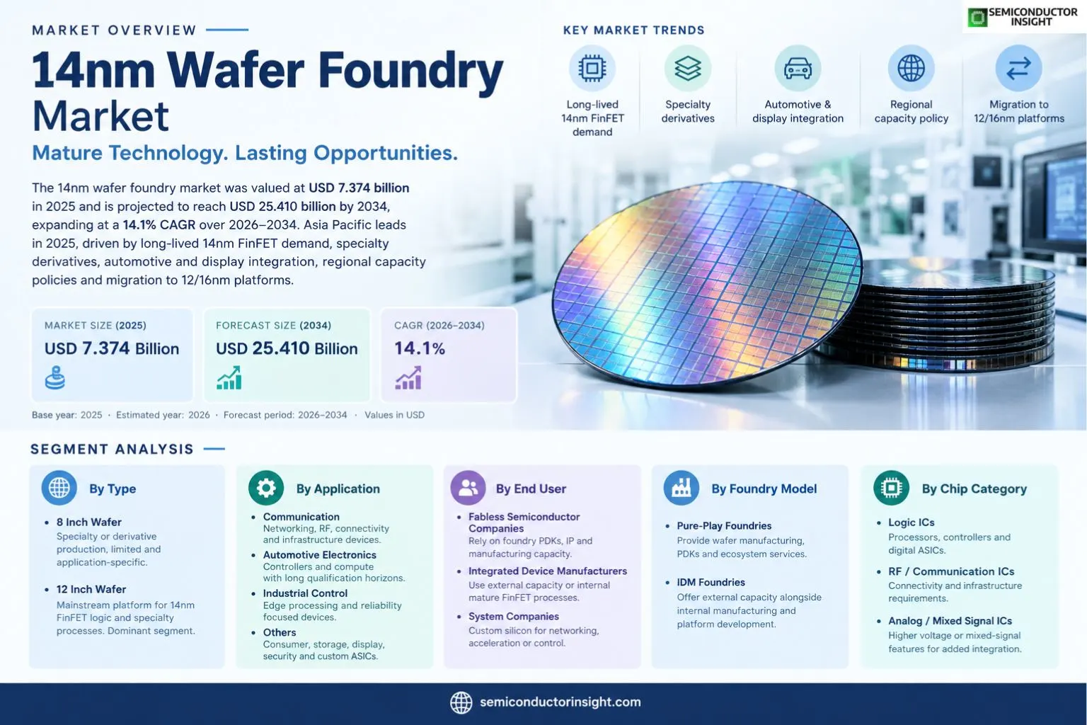
- Market size and growth: the market is valued at USD 7.374 billion in 2025 and is projected to reach USD 25.410 billion by 2034, representing a 14.1% CAGR over 2026–2034.
- 12 Inch Wafer leads by type because 300 mm manufacturing provides the mainstream economic platform for 14nm FinFET logic and derivative specialty processes at commercially relevant volume.
- Communication leads application demand because networking, RF, connectivity and infrastructure devices continue to use mature FinFET performance where leading-edge nodes are not economically necessary.
- Asia Pacific is the largest regional market, while Asia Pacific has the strongest incremental growth profile.
- Primary driver: mature FinFET economics, long product lifecycles and specialty 14nm derivatives sustain demand after leading-edge products have migrated to newer nodes
- Principal restraint: design migration, multi-patterning cost and competition from adjacent 12/16nm platforms limit growth for undifferentiated 14nm foundry capacity
Market Overview
The 14nm wafer foundry market was valued at USD 7.374 billion in 2025 and is projected to reach USD 25.410 billion by 2034, expanding at a 14.1% CAGR over 2026–2034. Asia Pacific leads in 2025, while the market is being reshaped by long-lived 14nm FinFET demand, 14nm specialty derivatives, automotive and display high-voltage integration, regional capacity policy and migration of some logic toward adjacent 12/16nm platforms.. For 14nm Wafer Foundry suppliers, the commercial implication is that product performance must translate into a measurable system benefit, not only a stronger component specification.
Fourteen-nanometer foundry technology remains commercially relevant because it combines FinFET transistor performance with a much more mature cost structure than leading-edge logic. Samsung states that its 14nm FinFET platform entered mass production in 2014 and continues to offer derivative logic and specialty technologies, while UMC operates a 14nm process with FinFET architecture for low-power and performance-oriented designs. GlobalFoundries has shipped millions of wafers across its FinFET platform since the middle of the last decade, demonstrating the long commercial tail that mature advanced nodes can sustain after their first consumer-processor generation.
The node is increasingly differentiated through application-specific derivatives rather than headline transistor scaling. Samsung’s specialty portfolio includes 14LPU-based embedded and RF-oriented options, while UMC announced a 14nm embedded high-voltage platform in May 2026 for display-driver and mixed-signal integration. These developments show how an established FinFET node can gain new demand when foundries add high-voltage, RF, automotive or nonvolatile features. Customers benefit because proven design rules and depreciated infrastructure can lower risk compared with migrating a moderate-complexity chip to a much newer process.
Geopolitics and supply resilience are also changing foundry economics. The U.S. Department of Commerce’s CHIPS award to GlobalFoundries supports expansion of current-generation manufacturing in New York and Vermont, while Asian foundries continue to hold the largest installed specialty and logic capacity. At the same time, TSMC’s adjacent N16/N12 family and other mature FinFET processes compete directly for designs that value ecosystem depth over an exact nominal node label. The market therefore includes both pure 14nm demand and a broader class of mature FinFET workloads selected on PDK maturity, IP, yield and regional capacity.
Segment Analysis: By Type
By type, the market is segmented into 8 Inch Wafer, 12 Inch Wafer. 12 Inch Wafer holds the leading position because 300 mm manufacturing provides the mainstream economic platform for 14nm FinFET logic and derivative specialty processes at commercially relevant volume. Procurement decisions in the 14nm Wafer Foundry market therefore increasingly consider qualification evidence, integration effort, lifecycle support and supply continuity alongside unit price. As adoption broadens, vendors that combine repeatable manufacturing with application engineering and documented reliability should be better positioned for long production programs.
| Type | Function / role | Market position |
|---|---|---|
| 8 Inch Wafer | Specialty or derivative 14nm-class production on smaller wafer formats is limited and application-specific. | Minor segment because mainstream FinFET economics favor larger wafer diameter. |
| 12 Inch Wafer | 300 mm FinFET manufacturing for logic, communication and derivative specialty devices. | Dominant type because leading 14nm foundry platforms were industrialized on 300 mm infrastructure. |
Commercial implications by type
Twelve-inch wafers dominate because 14nm FinFET requires expensive lithography, process control and multi-patterning that are economically matched to 300 mm fabs. The 8-inch category remains limited and is more relevant to specialized or transitional interpretations of node-class capability than to mainstream 14nm logic. For customers, wafer diameter is less important than available PDKs, qualified IP, design tools, mask cost, yield and long-term capacity. The market’s competitive center is therefore the mature 300 mm ecosystem rather than a broad split between wafer sizes.
Segment Analysis: By Application
By application, the market includes Communication, Automotive Electronics, Industrial Control, Others. Communication leads demand because networking, RF, connectivity and infrastructure devices continue to use mature FinFET performance where leading-edge nodes are not economically necessary. As adoption broadens, vendors that combine repeatable manufacturing with application engineering and documented reliability should be better positioned for long production programs. This makes design support and field-proven integration increasingly important because the cost of requalification can exceed the incremental saving from a lower-priced component.
| Application | Demand characteristics |
|---|---|
| Communication | Leading application across networking, wireless infrastructure, connectivity and selected RF or baseband devices. |
| Automotive Electronics | Controllers, networking and specialized compute benefit from mature FinFET performance with long qualification horizons. |
| Industrial Control | Edge processing, controllers and communication silicon use mature nodes where reliability and lifecycle outweigh maximum density. |
| Others | Consumer, storage, display, security and custom ASIC products sustain additional foundry demand. |
By End User
| End User | Commercial relevance |
|---|---|
| Fabless Semiconductor Companies | Rely on foundry PDKs, IP libraries and manufacturing capacity for 14nm products. |
| Integrated Device Manufacturers | Use external foundry capacity selectively or operate internal mature FinFET processes. |
| System Companies | Custom silicon programs may use mature FinFET nodes for networking, acceleration or control. |
By Foundry Model
| Foundry Model | Commercial relevance |
|---|---|
| Pure-Play Foundries | Provide wafer manufacturing, PDKs and ecosystem services without competing directly in most customer chip markets. |
| IDM Foundries | Offer external capacity alongside internal product manufacturing and platform development. |
By Chip Category
| Chip Category | Commercial relevance |
|---|---|
| Logic ICs | Processors, controllers and digital ASICs use 14nm FinFET density and performance. |
| RF / Communication ICs | Specialty derivatives support connectivity and infrastructure requirements. |
| Analog / Mixed Signal ICs | 14nm derivative processes add higher voltage or mixed-signal features where digital integration is valuable. |
Regional Analysis
Asia Pacific leads the market because Taiwan, South Korea and China contain the largest concentration of mature FinFET foundry capacity, fabless customers, semiconductor supply chains and 300 mm manufacturing infrastructure. Asia Pacific has the strongest growth profile through regional specialty derivatives, domestic semiconductor investment and continued demand for mature performance nodes are expanding qualified capacity across Asian foundries. This makes design support and field-proven integration increasingly important because the cost of requalification can exceed the incremental saving from a lower-priced component.
How does regional demand differ across this market?
Asia Pacific dominates installed 14nm-class foundry capacity through Samsung, UMC, SMIC and the broader Taiwan, South Korea and China semiconductor ecosystem. North America remains strategically important through GlobalFoundries, system companies and policy-supported domestic manufacturing, while Europe contributes automotive and industrial demand rather than large 14nm pure-play capacity. Other regions are mainly downstream consumers of chips fabricated elsewhere. The competitive geography is increasingly shaped by supply resilience and regional qualification because mature FinFET products often stay in production for many years and can be difficult to migrate between process platforms.
| Region | Position | Growth outlook | Demand profile | Supplier selection |
|---|---|---|---|---|
| Asia Pacific | Largest | Fastest | Foundry scale and semiconductor manufacturing | Yield, PDK maturity, capacity, cost |
| North America | Second | Strong | ASIC, defense, communications and domestic supply | Supply security, IP, long lifecycle |
| Europe | Third | Moderate | Automotive and industrial demand | Qualification, lifecycle, reliability |
| South America | Smaller | Selective | Downstream electronics | Cost and global supply access |
| Middle East & Africa | Emerging | Selective | Downstream systems and new semiconductor interest | Supply access, trusted manufacturing, cost |
Competitive Landscape
Competition is concentrated among foundries with proven FinFET yield, mature PDKs, qualified IP and enough 300 mm capacity to support long-lived customer programs. For 14nm Wafer Foundry suppliers, the commercial implication is that product performance must translate into a measurable system benefit, not only a stronger component specification. Procurement decisions in the 14nm Wafer Foundry market therefore increasingly consider qualification evidence, integration effort, lifecycle support and supply continuity alongside unit price. As adoption broadens, vendors that combine repeatable manufacturing with application engineering and documented reliability should be better positioned for long production programs.
Samsung established 14nm FinFET mass production in 2014 and continues to support logic and specialty derivatives, giving it a mature manufacturing and IP base. UMC competes through an established 14nm process and expanded the platform in 2026 with embedded high-voltage capability for display and mixed-signal applications. GlobalFoundries brings long-running FinFET manufacturing and a history of 14nm ASIC and AMD production. These suppliers compete less on a simple nominal node label than on yield, library quality, specialty options, design support and long-term manufacturing commitments.
SMIC has built domestic Chinese 14nm capability and reports first-generation mass production beginning in 2019, while additional derivative platforms extend China’s mature advanced-node ecosystem. This capacity is strategically important for local fabless customers that want domestic manufacturing options, even though equipment restrictions and process access affect expansion. Regional foundries also compete against adjacent nodes rather than only exact 14nm. TSMC’s N16 and N12 platforms, for example, provide mature FinFET alternatives with extensive IP, meaning customers can choose a neighboring node when ecosystem depth or qualified capacity outweighs nominal geometry.
Foundry choice is unusually sticky at 14nm because customers invest heavily in physical design, timing closure, IP qualification, masks and reliability testing. Moving the same product to another foundry often requires substantial redesign even when the nominal node is similar. This protects incumbent design wins but raises customer concern about supply concentration. Public investment in domestic manufacturing, including U.S. support for GlobalFoundries, reflects the strategic importance of long-lived current-generation capacity. Suppliers that offer multi-site continuity, transparent lifecycle policy and specialty derivatives can therefore compete on supply assurance as much as wafer performance.
| Competitive tier | Representative participants | Competitive focus |
|---|---|---|
| Established 14nm FinFET foundries | Samsung, GlobalFoundries, UMC | Mature 300 mm manufacturing, PDKs and specialty derivatives |
| Regional mature-node challengers | SMIC and Chinese foundries | Domestic capacity and local fabless ecosystems |
| Adjacent-node competitors | TSMC N16/N12, Intel and other mature FinFET platforms | Substitute process options with broad IP and manufacturing support |
Companies Profiled
Samsung Foundry, GlobalFoundries, UMC, SMIC, Hua Hong Semiconductor, Tower Semiconductor, Intel Foundry, TSMC. The set reflects companies directly active in products, process technology, manufacturing or the supporting application ecosystem rather than an evaluative ranking. Procurement decisions in the 14nm Wafer Foundry market therefore increasingly consider qualification evidence, integration effort, lifecycle support and supply continuity alongside unit price. As adoption broadens, vendors that combine repeatable manufacturing with application engineering and documented reliability should be better positioned for long production programs.
Production Capacity Analysis
Capacity depends on qualified 300 mm FinFET fabs, multi-patterning lithography, mature process-control recipes, mask infrastructure, IP libraries, backend test and enough long-term wafer allocation to support products that can remain active for a decade. For 14nm Wafer Foundry suppliers, the commercial implication is that product performance must translate into a measurable system benefit, not only a stronger component specification. Procurement decisions in the 14nm Wafer Foundry market therefore increasingly consider qualification evidence, integration effort, lifecycle support and supply continuity alongside unit price.
Fourteen-nanometer manufacturing requires many more lithography and process-control steps than older planar nodes, so capacity cannot be added as cheaply as mature 28nm or 40nm production. Most commercial 14nm platforms use 300 mm wafers and FinFET devices, requiring advanced etch, deposition and multi-patterning capability. The advantage today is process maturity: tools, recipes and yield learning have accumulated over many years. Foundries can therefore focus on debottlenecking, specialty modules and stable long-term production rather than the rapid yield ramp that characterized the node’s first commercial generation.
Effective capacity also depends on customer qualification and design ecosystem. A fab may have available wafer starts, but a customer still needs compatible standard cells, SRAM, interfaces, analog IP, EDA flows and package options before tape-out. Automotive or long-life industrial designs add reliability qualification that can tie a product to one process for many years. U.S. and Asian capacity investments therefore matter not only because they add physical wafers but because they preserve experienced engineering teams, mask flows, test programs and PDK support that existing 14nm products need throughout their lifecycle.
Market Dynamics
The market is transitioning from mainstream leading-edge logic toward a mature FinFET specialty and lifecycle node used where performance remains sufficient and ecosystem stability outweighs maximum transistor density. For 14nm Wafer Foundry suppliers, the commercial implication is that product performance must translate into a measurable system benefit, not only a stronger component specification. Procurement decisions in the 14nm Wafer Foundry market therefore increasingly consider qualification evidence, integration effort, lifecycle support and supply continuity alongside unit price.
The 14nm node no longer competes for every flagship processor, but that does not eliminate demand. Networking, communications, industrial, automotive and custom ASIC products can achieve their required performance without paying leading-edge mask and wafer costs. Foundries are extending the platform with specialty capabilities such as embedded high voltage or RF-oriented device options, which opens new use cases and improves fab utilization. Competition from 12nm and 16nm derivatives remains intense, so sustainable growth depends on differentiated process features, capacity assurance and customer migration cost rather than generic logic density.
Market Drivers
Drivers Impact Analysis
| Driver | Impact | Commercial mechanism |
|---|---|---|
| Mature FinFET economics | High | Fourteen-nanometer technology offers substantially more transistor density and performance than older planar nodes while benefiting from years of yield learning and depreciated infrastructure. For communications, industrial and custom ASICs, the node can deliver sufficient compute without the very high mask, IP and wafer cost associated with leading-edge processes. This creates a durable middle market where customers value predictable yield, stable PDKs and known reliability. Long-lived products can amortize design cost over many years, making a mature FinFET platform economically attractive even as newer nodes continue scaling. |
| Specialty process derivatives | High | Foundries can extend mature 14nm infrastructure into new applications by adding device options that are not available on the original logic platform. UMC’s 2026 embedded high-voltage development is a clear example, targeting display and mixed-signal integration that combines FinFET logic with higher-voltage functions. Samsung also lists specialty 14nm derivatives for RF and embedded applications. These additions increase addressable demand without requiring a completely new fab generation, improving asset utilization and giving customers a path to integrate digital control with application-specific analog or high-voltage functions. |
| Automotive and industrial lifecycle | Medium | Vehicles and industrial systems often require semiconductors to remain available for many years, favoring mature nodes with stable process control and long-term support. Fourteen-nanometer FinFET can provide more computing headroom than older planar technologies while avoiding the cost and rapid change of leading-edge nodes. The challenge is qualification: automotive products require extensive reliability testing and may remain tied to one foundry for a decade. Once qualified, however, these programs create sticky wafer demand and reward suppliers that maintain process continuity, documentation and traceability. |
| Regional supply resilience | Medium | Governments and system companies increasingly value semiconductor capacity that is geographically diversified and available for strategic products. U.S. CHIPS support for GlobalFoundries highlights the policy importance of current-generation manufacturing, while Asian countries continue investing in domestic semiconductor ecosystems. Fourteen-nanometer technology is advanced enough for many communications, defense and infrastructure applications but mature enough to support longer manufacturing commitments. Customers may accept a modest cost premium when regional capacity reduces supply risk, export uncertainty or dependence on one geographic manufacturing cluster. |
Mature FinFET economics
Fourteen-nanometer technology offers substantially more transistor density and performance than older planar nodes while benefiting from years of yield learning and depreciated infrastructure. For communications, industrial and custom ASICs, the node can deliver sufficient compute without the very high mask, IP and wafer cost associated with leading-edge processes. This creates a durable middle market where customers value predictable yield, stable PDKs and known reliability. Long-lived products can amortize design cost over many years, making a mature FinFET platform economically attractive even as newer nodes continue scaling.
Specialty process derivatives
Foundries can extend mature 14nm infrastructure into new applications by adding device options that are not available on the original logic platform. UMC’s 2026 embedded high-voltage development is a clear example, targeting display and mixed-signal integration that combines FinFET logic with higher-voltage functions. Samsung also lists specialty 14nm derivatives for RF and embedded applications. These additions increase addressable demand without requiring a completely new fab generation, improving asset utilization and giving customers a path to integrate digital control with application-specific analog or high-voltage functions.
Automotive and industrial lifecycle
Vehicles and industrial systems often require semiconductors to remain available for many years, favoring mature nodes with stable process control and long-term support. Fourteen-nanometer FinFET can provide more computing headroom than older planar technologies while avoiding the cost and rapid change of leading-edge nodes. The challenge is qualification: automotive products require extensive reliability testing and may remain tied to one foundry for a decade. Once qualified, however, these programs create sticky wafer demand and reward suppliers that maintain process continuity, documentation and traceability.
Regional supply resilience
Governments and system companies increasingly value semiconductor capacity that is geographically diversified and available for strategic products. U.S. CHIPS support for GlobalFoundries highlights the policy importance of current-generation manufacturing, while Asian countries continue investing in domestic semiconductor ecosystems. Fourteen-nanometer technology is advanced enough for many communications, defense and infrastructure applications but mature enough to support longer manufacturing commitments. Customers may accept a modest cost premium when regional capacity reduces supply risk, export uncertainty or dependence on one geographic manufacturing cluster.
Market Restraints
Restraints Impact Analysis
| Restraint | Impact | Commercial mechanism |
|---|---|---|
| Adjacent-node competition | High | Customers do not always distinguish sharply between 14nm, 16nm and 12nm labels because actual performance depends on process generation, libraries and design rules. TSMC’s mature N16/N12 platforms and other FinFET alternatives compete for the same networking, industrial and custom logic products. A foundry with stronger IP, better yield or more available capacity can win even if the nominal geometry differs. This limits pricing power for undifferentiated 14nm capacity and pushes suppliers toward specialty derivatives, customer-specific support or regional supply advantages. |
| High mask and design cost | High | Although 14nm is mature, it still uses complex multi-patterning and FinFET design rules that make masks and physical design much more expensive than older planar nodes. Small-volume industrial or regional custom chips may find 28nm or 40nm economically preferable if performance requirements are modest. The fixed design cost means the 14nm market favors products with sufficient lifetime volume or system value. Shuttle programs and reusable IP can reduce the barrier, but the node remains too expensive for many low-volume ASIC projects. |
| Foundry migration difficulty | Medium | A chip designed for one 14nm foundry is not portable to another by simply changing masks. Transistor models, standard cells, SRAM, analog IP, design rules and timing behavior differ, so migration can require substantial physical redesign and requalification. This creates customer lock-in after tape-out but also increases procurement risk if capacity or geopolitical conditions change. Companies seeking second-source resilience may need to design separate implementations or choose a supplier with multi-site capability, adding cost and time before volume production begins. |
| Leading-edge migration | Medium | Applications that need maximum AI performance, very high transistor density or energy efficiency continue moving to smaller process nodes, reducing 14nm share in flagship compute. Mature FinFET growth therefore cannot rely on the same processors that initially drove the node. Foundries must capture communications, automotive, industrial, display and specialty logic where performance requirements are more stable. If newer nodes become much cheaper or older planar nodes add enough capability, 14nm can be squeezed between leading-edge performance and mature-node cost, making differentiation essential. |
Adjacent-node competition
Customers do not always distinguish sharply between 14nm, 16nm and 12nm labels because actual performance depends on process generation, libraries and design rules. TSMC’s mature N16/N12 platforms and other FinFET alternatives compete for the same networking, industrial and custom logic products. A foundry with stronger IP, better yield or more available capacity can win even if the nominal geometry differs. This limits pricing power for undifferentiated 14nm capacity and pushes suppliers toward specialty derivatives, customer-specific support or regional supply advantages.
High mask and design cost
Although 14nm is mature, it still uses complex multi-patterning and FinFET design rules that make masks and physical design much more expensive than older planar nodes. Small-volume industrial or regional custom chips may find 28nm or 40nm economically preferable if performance requirements are modest. The fixed design cost means the 14nm market favors products with sufficient lifetime volume or system value. Shuttle programs and reusable IP can reduce the barrier, but the node remains too expensive for many low-volume ASIC projects.
Foundry migration difficulty
A chip designed for one 14nm foundry is not portable to another by simply changing masks. Transistor models, standard cells, SRAM, analog IP, design rules and timing behavior differ, so migration can require substantial physical redesign and requalification. This creates customer lock-in after tape-out but also increases procurement risk if capacity or geopolitical conditions change. Companies seeking second-source resilience may need to design separate implementations or choose a supplier with multi-site capability, adding cost and time before volume production begins.
Leading-edge migration
Applications that need maximum AI performance, very high transistor density or energy efficiency continue moving to smaller process nodes, reducing 14nm share in flagship compute. Mature FinFET growth therefore cannot rely on the same processors that initially drove the node. Foundries must capture communications, automotive, industrial, display and specialty logic where performance requirements are more stable. If newer nodes become much cheaper or older planar nodes add enough capability, 14nm can be squeezed between leading-edge performance and mature-node cost, making differentiation essential.
Market Opportunities
Embedded high-voltage integration
UMC’s 2026 14nm eHV announcement demonstrates a route to combine dense FinFET digital logic with higher-voltage functions for display and mixed-signal products. Integrating these blocks can reduce die count, power and board complexity compared with using a separate digital controller and high-voltage device. Similar specialty extensions could address sensors, power control and interface ICs. The opportunity is attractive because it reuses mature 300 mm infrastructure while creating differentiated functionality that neighboring generic logic nodes may not offer with the same qualified ecosystem.
Automotive ASICs
Software-defined vehicles, networking, domain control and sensor processing require more compute than many legacy automotive MCUs can deliver, but not every function needs a leading-edge process. Fourteen-nanometer FinFET can provide a mature compromise for custom controllers or networking ASICs if foundries support automotive qualification and long supply life. The design cost is high, so the best candidates are high-volume vehicle platforms or reusable silicon that serves several models. Once qualified, long platform lifecycles can create durable wafer demand.
Communications and infrastructure silicon
Switching, baseband, security and networking devices often remain in production for years and can use mature FinFET when bandwidth or power needs exceed planar nodes. Communication applications already lead the market and benefit from extensive high-speed interface IP developed during the node’s mainstream years. Foundries can extend demand by maintaining SerDes, PCIe, DDR and networking libraries alongside stable wafer capacity. These products value predictable supply and design reuse, particularly when telecom infrastructure qualification makes frequent process migration undesirable.
Trusted regional manufacturing
Strategic customers increasingly evaluate where semiconductors are fabricated and whether capacity can be maintained during supply disruptions or geopolitical shocks. Mature FinFET nodes are relevant because they support sophisticated logic without requiring the newest lithography tools. Public incentives and domestic-capacity programs can make regional 14nm-class manufacturing economically viable for defense, communications and infrastructure customers. Suppliers that combine geographic diversity with mature PDKs and long lifecycle commitments can capture programs where secure availability is worth more than the absolute lowest wafer price.
Supply Chain Analysis
EDA, PDKs, IP libraries and verification
300 mm FinFET, lithography, etch and deposition
Advanced masks, photoresist, gases and process chemicals
Assembly, qualification, reliability and system integration
Design ecosystem
A mature 14nm foundry platform depends on much more than transistor models. Customers need standard-cell libraries, SRAM, high-speed interfaces, analog IP, design-rule checking, extraction and signoff flows that have been validated across many tape-outs. This ecosystem is one reason established nodes persist for years after newer technology becomes available. Foundries with broad third-party IP and EDA certification can reduce schedule risk substantially, while a technically capable process with a weak ecosystem may struggle to attract fabless customers that cannot afford to develop every interface internally.
Wafer fabrication
Commercial 14nm FinFET uses 300 mm manufacturing with complex deposition, etch and lithography sequences to form three-dimensional transistor structures and dense interconnects. Multi-patterning increases process steps and cycle time relative to older planar nodes, but mature fabs benefit from many years of yield learning. Equipment uptime, defect control and recipe stability are therefore key competitive factors. Capacity expansion is often achieved through tool additions and debottlenecking rather than a completely new greenfield fab, which can improve returns while preserving customer-qualified process conditions.
Mask & materials
Fourteen-nanometer designs require advanced mask sets and tightly controlled photoresist, gases, deposition precursors and clean materials across many patterning layers. The high mask-set cost contributes to substantial non-recurring engineering, especially for smaller ASIC customers. Supply continuity matters because changing a process chemical or mask flow can require foundry requalification and potentially affect device characteristics. Mature nodes benefit from established material supply and process recipes, but geopolitical restrictions or vendor concentration can still influence expansion plans and the geographic availability of certain manufacturing capabilities.
Packaging & test
After wafer fabrication, many 14nm products use advanced BGA, flip-chip or other high-pin-count packages that must preserve signal integrity and thermal performance. Networking and automotive chips can require long reliability testing, high-speed interface characterization and customer-specific package qualification. The backend is generally less node-specific than wafer fabrication but can still constrain launch schedules when substrates or test capacity are tight. Customers increasingly evaluate the full manufacturing path, including assembly geography and long-term test support, when selecting a foundry for products expected to remain active for many years.
Recent Developments
May 2026 — UMC announces 14nm embedded high-voltage platform
The new 14nm eHV platform extends mature FinFET manufacturing into display and mixed-signal applications requiring higher-voltage device integration. Source
Current — Samsung continues 14nm logic and specialty process support
Samsung’s current foundry materials retain 14nm FinFET among established logic nodes with derivative specialty technologies. Source
Current — GlobalFoundries maintains mature FinFET manufacturing
GlobalFoundries positions its FinFET platform as a long-running technology with millions of wafers shipped and multiple application markets. Source
Report Scope & Segmentation
| Attribute | Coverage |
|---|---|
| Market | 14nm Wafer Foundry |
| Base Year | 2025 |
| Estimated Year | 2026 |
| Forecast Period | 2026–2034 |
| 2025 Market Size | USD 7.374 billion |
| 2026 Estimated Size | USD 8.830 billion |
| 2034 Forecast Size | USD 25.410 billion |
| CAGR | 14.1% (2026–2034) |
| By Type | 8 Inch Wafer, 12 Inch Wafer |
| By Application | Communication, Automotive Electronics, Industrial Control, Others |
| By End User | Fabless Semiconductor Companies, Integrated Device Manufacturers, System Companies |
| By Foundry Model | Pure-Play Foundries, IDM Foundries |
| By Chip Category | Logic ICs, RF / Communication ICs, Analog / Mixed Signal ICs |
| Regions | Asia Pacific, North America, Europe, South America, Middle East & Africa |
| Companies Profiled | Samsung Foundry, GlobalFoundries, UMC, SMIC, Hua Hong Semiconductor, Tower Semiconductor, Intel Foundry, TSMC |
Frequently Asked Questions
What is the 14nm wafer foundry market size in 2025?
The market is valued at USD 7.374 billion in 2025.
What is the projected market size by 2034?
The market is projected to reach USD 25.410 billion by 2034.
What is the CAGR from 2026 to 2034?
The market is expected to expand at a 14.1% CAGR.
Which region leads the market?
Asia Pacific is the largest regional market in 2025.
Which type leads the market?
12 Inch Wafer is the leading type.
Which application leads demand?
Communication is the leading application.
What is the main growth driver?
mature FinFET economics, long product lifecycles and specialty 14nm derivatives sustain demand after leading-edge products have migrated to newer nodes.
What is the principal restraint?
design migration, multi-patterning cost and competition from adjacent 12/16nm platforms limit growth for undifferentiated 14nm foundry capacity.
Where are the strongest opportunities?
14nm embedded high-voltage, automotive ASICs, communications silicon, secure domestic capacity and long-life industrial products.
Which companies are active in the market?
Samsung Foundry, GlobalFoundries, UMC, SMIC, Hua Hong Semiconductor, Tower Semiconductor, Intel Foundry, TSMC.
Research Sources & Evidence Base
View primary, official and technical evidence used in this overview
- Samsung Foundry: Logic Node Technology — 14nm FinFET mass-production history and current mature-node positioning.
- Samsung Foundry: Company Information — Foundry platform history, capacity and technology evolution.
- Samsung Foundry: Specialty Technology — 14nm specialty derivatives for embedded and RF-oriented applications.
- UMC: 14nm Technology — Current 14nm FinFET platform characteristics and foundry positioning.
- UMC: 14nm Embedded High-Voltage Platform — 2026 expansion of 14nm into embedded high-voltage applications.
- UMC: 14nm Mass Production Milestone — Historical qualification and volume-manufacturing evidence.
- GlobalFoundries: FinFET Technology — Current mature FinFET platform and cumulative wafer-production context.
- GlobalFoundries: 14nm FinFET AMD Milestone — Historical 14nm production and customer qualification evidence.
- GlobalFoundries: 14nm ASIC Offering — 14nm ASIC manufacturing and design-ecosystem evidence.
- GlobalFoundries: 14nm Design Infrastructure — PDK, IP and EDA ecosystem development for 14nm customers.
- U.S. Department of Commerce: CHIPS Incentives Award to GlobalFoundries — Policy support for U.S. current-generation semiconductor capacity and supply resilience.
- TSMC: N16/N12 Data Center & Compute Platform — Adjacent mature FinFET technology competing for similar long-life and infrastructure designs.
Get Sample Report PDF for Exclusive Insights
Report Sample Includes
- Table of Contents
- List of Tables & Figures
- Charts, Research Methodology, and more...
 Download Sample Report PDF