
CdZnTe Crystal Market Insights
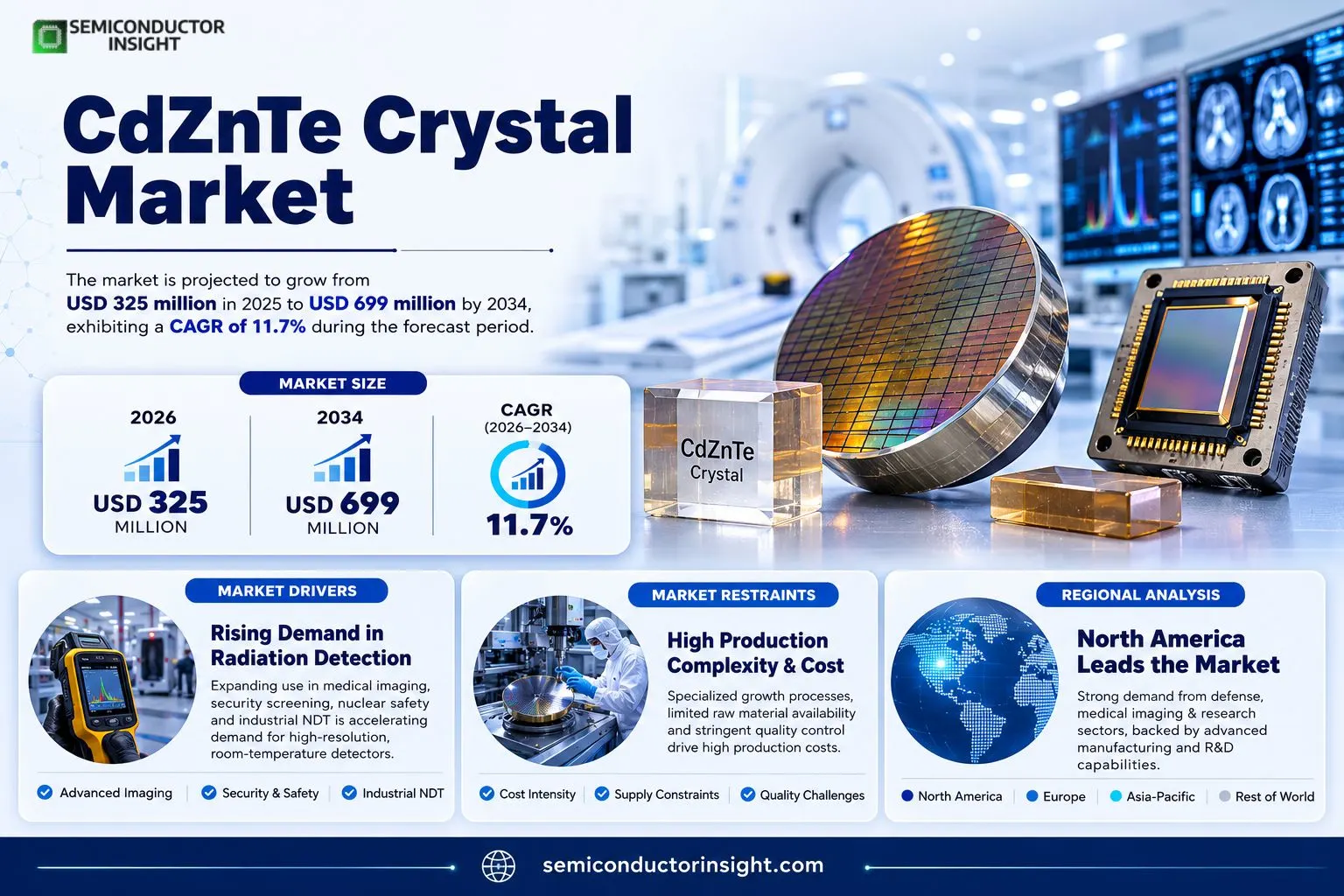
CdZnTe Crystal market size was valued at USD 325 million in 2025. The market is expected to reach USD 699 million by 2034, reflecting a compound annual growth rate of 11.7% over the forecast horizon.
Cadmium‑zinc‑telluride (CdZnTe) crystal is a II‑VI compound semiconductor formed from cadmium telluride and zinc telluride. It encompasses ingots, wafers, substrates, detector crystals, sensor chips and integrated detector modules. Its principal advantage lies in direct conversion of high‑energy photonssuch as X‑rays and gamma raysinto electrical signals at room temperature, delivering high detection efficiency, superior energy resolution and fine spatial resolution without requiring cryogenic cooling.The material finds core use in medical imaging systems (including photon‑counting CT and SPECT), security inspection equipment, infrared focal‑plane detector substrates and industrial non‑destructive testing devices because it combines high atomic number with a wide bandgap that enables compact, low‑maintenance detectors.
MARKET DRIVERS
Rising Demand in Radiation Detection
The surge in security screening and nuclear safety initiatives has elevated the need for high‑resolution detectors. **CdZnTe** crystals, owing to their superior energy resolution at room temperature, are becoming the preferred sensor material, prompting OEMs to expand capacity and invest in dedicated lines.
Advances in Material Synthesis
Recent breakthroughs in vertical gradient freezing and liquid‑phase epitaxy have trimmed defect density, translating into longer device lifespans. These technical gains reduce total cost of ownership for end‑users, encouraging broader adoption across medical imaging and industrial gauging.
➤ “The convergence of tighter safety regulations and lower‑cost crystal growth is reshaping the CdZnTe landscape.”
Collectively, the regulatory push and material‑science progress form a twin‑engine that accelerates the **CdZnTe Crystal Market**, positioning it as a strategic commodity for next‑generation detection solutions.
MARKET CHALLENGES
Manufacturing Complexity
Producing defect‑free CdZnTe crystals demands precise temperature gradients and ultra‑clean environments. Even minor fluctuations can introduce dislocation networks that impair detector performance, forcing manufacturers to adopt costly quality‑control regimes.
Other Challenges
Supply Chain Vulnerabilities
The reliance on high‑purity cadmium, zinc, and tellurium concentrates risk in a limited number of mineral producers. Geopolitical tensions or mining disruptions can quickly translate into material shortages, inflating lead times for crystal growers.
MARKET RESTRAINTS
High Production Cost
Unlike silicon, CdZnTe requires specialized crucibles and prolonged annealing cycles, driving unit costs well above those of conventional semiconductors. This price premium limits market penetration in price‑sensitive segments such as consumer‑grade radiation monitors.Furthermore, the capital intensity of crystal‑growth facilities creates a barrier to entry, constraining the number of players able to scale production efficiently and keep prices competitive.
MARKET OPPORTUNITIES
Emerging Applications in Space Exploration
Space agencies are evaluating CdZnTe detectors for gamma‑ray spectroscopy on deep‑space missions because the material operates reliably across extreme temperature ranges without active cooling. This niche, though small today, could generate a stable demand stream as launch frequencies increase.Parallel advancements in miniaturized readout electronics are unlocking new form factors, enabling integration of CdZnTe sensors into handheld spectrometers for field geologists and first responders, thereby widening the addressable market beyond traditional industrial users.
CdZnTe Crystal Market Trends
Room‑Temperature Photon Conversion Gains Traction
The ability of CdZnTe crystals to transform high‑energy photons into charge carriers at ambient temperature is reshaping detector design across several high‑value segments. By eliminating cryogenic cooling, manufacturers can reduce system mass, lower maintenance cycles, and introduce multi‑energy imaging without the penalty of bulky thermal management. Medical‑imaging OEMs are leveraging this attribute to launch photon‑counting CT scanners that promise dose reductions and material discrimination, while research labs adopt compact spectrometers for elemental analysis. The cumulative effect is a shift from pure material sales toward bundled solutions that embed crystal growth, pixelated sensors, and ASIC read‑out in a single offering, driving higher‑margin contracts and tighter supplier relationships. As OEMs transition to these integrated platforms, supply chains are compelled to synchronize crystal growth schedules with ASIC design cycles, a coordination that intensifies the importance of predictive yield modeling and long‑term qualification programs. Consequently, the pricing dynamics reflect a premium for reliability and on‑time delivery, reshaping contract negotiations across the value chain.
Other Trends
Infrared Substrate Dynamics
Infrared focal‑plane manufacturers place stringent demands on CdZnTe substrates, where lattice matching and zinc‑content control dictate detector performance. Low‑zinc compositions that align with HgCdTe epitaxy reduce dislocation density and preserve infrared transmittance, making wafer uniformity a decisive purchasing factor. Customers prioritize large‑diameter blanks with sub‑nanometer surface roughness, because polishing steps translate directly into focal‑plane yield. As semiconductor fabs migrate toward 6‑inch and 8‑inch formats, suppliers that can guarantee batch‑to‑batch compositional stability gain preferential access to long‑term contracts. Consequently, the substrate stream is witnessing incremental price premiums for crystals that meet tight tolerances, while vendors expand from raw ingot delivery to value‑added services such as metrology certification and custom polishing.
Security and Nuclear Detection Demand Accelerates
Security inspection and nuclear‑safety platforms are the primary carriers of demand for radiation‑detection modules built around CdZnTe crystals. Portable gamma‑ray imagers benefit from the material’s high resistivity and low leakage, enabling extended field deployments without the logistical burden of liquid‑nitrogen cooling. Operators in border‑control, decommissioning, and emergency‑response sectors prioritize devices that combine fine‑pixel arrays with robust ASIC interfaces, because these characteristics translate into rapid material discrimination and reliable alarm thresholds. Suppliers that integrate crystal growth with detector packaging therefore command premium pricing, while also facing pressure to sustain high‑yield production across multiple form factors. The emerging emphasis on turnkey spectroscopic solutions suggests that future contracts will increasingly bundle crystal supply, detector calibration, and software analytics, reshaping the revenue model of CdZnTe Crystal Market toward service‑centric arrangements.
COMPETITIVE LANDSCAPEKey Industry Players
Competitive overview of the CdZnTe crystal sector
CdZnTe Crystal Market is anchored by a handful of vertically integrated firms that combine crystal growth, detector fabrication, and application‑specific module assembly. The most dominant player, Redlen Technologies, leverages proprietary Bridgman‑modified growth lines to deliver large‑area, low‑defect wafers that satisfy the stringent resistivity and leakage‑current specifications demanded by photon‑counting CT and homeland‑security scanners. Its ability to guarantee multi‑kilogram volume shipments under long‑term supply contracts forces smaller entrants to focus on niche customisation or downstream electronics, reinforcing a tiered market structure where scale and defect‑control competence dictate pricing power.Beyond the market leader, a diverse set of specialists competes on technology depth or regional advantage. Kromek Group and Vital Materials have expanded from raw crystal provision to fully packaged detector arrays, capitalising on the surge in portable gamma spectrometry. Japanese and Chinese suppliers such as JX Advanced Metals and Shaanxi Imdetek concentrate on low‑zinc substrates for MCT infrared focal‑plane devices, exploiting proximity to major infrared camera manufacturers. European outfits like Mirion Technologies and CapeSym focus on high‑resolution nuclear‑medicine modules, while firms such as H3D, Inc. and X‑Z LAB, Inc. differentiate through ASIC‑centric readout integration that enables ultra‑fine pixel pitches. This mosaic of capabilities creates a competitive environment where expertise in crystal uniformity, pixelisation, and system integration outweighs simple commodity pricing.
List of Key CdZnTe Crystal Companies Profiled
- Redlen Technologies
- Kromek Group
- JX Advanced Metals Corporation
- Vital Materials
- Shaanxi Imdetek Co., Ltd.
- H3D, Inc.
- X‑Z LAB, Inc.
- Mirion Technologies, Inc.
- American Elements
- Prosun Semiconductor Limited
- 5N Plus Inc.
- Due2Lab S.r.l.
- Hangzhou Shalom Electro‑optics Technology Co., Ltd.
- CrystalsNord LLC
- Eurorad S.A.
Segment Analysis:
| Segment Category | Sub-Segments | Key Insights |
| By Type |
|
Raw Crystals & Wafers dominate early‑stage value creation and drive downstream differentiation.
|
| By Application |
|
Medical Imaging is the leading application due to the compelling need for energy‑resolved, low‑dose imaging.
|
| By End User |
|
Medical equipment manufacturers lead end‑user demand, shaping product specifications.
|
| By Technology |
|
Advanced pixelation & ASIC integration is the decisive technology for high‑performance detectors.
|
| By Value Chain |
|
System integration is emerging as the highest‑value segment.
|
Regional Analysis: CdZnTe Crystal Market
North America
Suppliers have diversified sourcing of high‑purity cadmium, zinc, and tellurium, reducing exposure to single‑point failures. Collaborative agreements with raw‑material miners allow manufacturers to lock in pricing and ensure continuity, a critical factor as detector projects scale.
The FDA’s guidance on medical imaging devices and the DoD’s stringent qualification processes compel producers to adopt robust quality‑management systems. Clear criteria for crystal defect thresholds streamline certification timelines.
End‑users prioritize stability under varied temperature cycles and low leakage currents. This preference pushes manufacturers toward refined growth techniques that minimize dislocation densities, influencing material‑selection decisions across aerospace and health sectors.
Research clusters around MIT, Stanford and the University of Arizona host joint labs where academia and industry test novel doping strategies, accelerating the translation of lab‑scale breakthroughs into commercial crystal batches.
Europe
European stakeholders draw strength from a coordinated funding landscape that links Horizon Europe grants to semiconductor research. The emphasis on sustainable manufacturing has prompted firms to explore closed‑loop recycling of tellurium, aligning supply considerations with environmental commitments. Market participants note that aerospace customers value the material’s radiation hardness, which fuels niche but stable orders. Meanwhile, regulatory harmonization across the EU simplifies cross‑border certification, allowing mid‑size producers to expand without duplicative testing procedures.
Asia‑Pacific
In the Asia‑Pacific corridor, rapid expansion of satellite constellations and security surveillance infrastructure is reshaping demand patterns for CdZnTe crystals. Nations such as Japan and South Korea invest heavily in indigenously sourced semiconductor capabilities, fostering a home‑grown supplier base that reduces reliance on imports. Local manufacturers are adapting crystal growth cycles to accommodate higher throughput, while maintaining the defect control required for space‑grade detectors. The region’s cost‑competitiveness, coupled with rising technical proficiency, positions it as an emerging source of both material and application expertise.
South America
South American markets are still nascent in the CdZnTe domain, yet the presence of abundant tellurium mining in Chile offers a strategic advantage. Companies are exploring joint ventures that couple mining expertise with crystal‑growth facilities, aiming to capture value downstream. While end‑user demand remains limited, growing interest in radiation monitoring for mining safety and environmental assessment suggests a gradual build‑up of localized consumption.
Middle East & Africa
The Middle East and Africa region presents a mixed picture. Investment in scientific research hubs, particularly in the United Arab Emirates, has sparked preliminary studies into high‑energy detection for oil‑field monitoring. African nations, leveraging their mineral wealth, are beginning to assess the feasibility of processing cadmium and zinc locally. Though commercial volumes are modest, the strategic intent to develop a self‑sufficient supply chain is evident, setting the stage for future market entry as technology readiness improves.
Report Scope
This market research report provides a comprehensive analysis of the CdZnTe Crystal Market , covering the forecast period 2026–2034. It offers detailed insights into market dynamics, technological advancements, competitive landscape, and key trends shaping the industry.
Key focus areas of the report include:
-
Market Overview: The report begins with an overview outlining its current market scenario, key growth indicators, and industry transformation drivers. It discusses macroeconomic factors, demand–supply balance, regulatory landscape, and the strategic role of semiconductors in powering advancements across industries such as automotive, telecommunications, consumer electronics, and industrial automation.
- Market Size & Forecast: Historical data and future projections for revenue, unit shipments, and market value across major regions and segments.
- Segmentation Analysis: Detailed breakdown by product type, technology, application, and end-user industry to identify high-growth segments and investment opportunities.
- Regional Insights: Insights into market performance across North America, Europe, Asia-Pacific, Latin America, and the Middle East & Africa, including country-level analysis where relevant.
- Competitive Landscape: Profiles of leading market participants, including their product offerings, R&D focus, manufacturing capacity, pricing strategies, and recent developments such as mergers, acquisitions, and partnerships.
- Technology Trends & Innovation: Assessment of emerging technologies, integration of AI/IoT, semiconductor design trends, fabrication techniques, and evolving industry standards.
- Market Drivers & Restraints: Evaluation of factors driving market growth along with challenges, supply chain constraints, regulatory issues, and market-entry barriers.
- Stakeholder Insights: Insights for component suppliers, OEMs, system integrators, investors, and policymakers regarding the evolving ecosystem and strategic opportunities.
Primary and secondary research methods are employed, including interviews with industry experts, data from verified sources, and real-time market intelligence to ensure the accuracy and reliability of the insights presented.
FREQUENTLY ASKED QUESTIONS:
What is the current market size of CdZnTe Crystal Market?
-> CdZnTe Crystal Market was valued at USD 325 million in 2025 and is expected to reach USD 699 million by 2034, growing at a CAGR of 11.7% during the forecast period.
Which key companies operate in CdZnTe Crystal Market?
-> Key players include Canon Inc., Kromek Group, ASELSAN, JX Advanced Metals Corporation, Shaanxi Imdetek Co., Ltd., Kinheng Crystal Materials (Shanghai) Co., Ltd., Western Minmetals (SC) Corporation, Prosun Semiconductor Limited, Vital Materials, CapeSym, Inc., H3D, Inc., X‑Z LAB, Inc., Mirion Technologies, Inc., Stanford Advanced Materials, American Elements, Radiation Detection Technologies, Inc., MTI Corporation, 5N Plus Inc., Due2Lab S.r.l., ZRF Ritec SIA, Baltic Scientific Instruments, Ltd., Eurorad S.A., CrystalsNord LLC, Hangzhou Shalom Electro‑optics Technology Co., Ltd.
What are the key growth drivers?
-> Key growth drivers include the unique ability of CdZnTe to directly convert high‑energy photons at room temperature, increasing demand in medical imaging (photon‑counting CT, SPECT), security inspection, nuclear safety, and industrial non‑destructive testing, as well as ongoing advancements in crystal‑growth technologies that improve yield and defect control.
Which region dominates the market?
-> North America currently holds the largest share of CdZnTe Crystal Market, driven by strong demand from defense, security, and medical imaging sectors, while Europe and Asia‑Pacific show rapid growth trajectories.
What are the emerging trends?
-> Emerging trends include the integration of CdZnTe crystals into fully packaged detector modules and photon‑counting imaging systems, development of fine‑pixel ASIC readouts, and expansion of applications in portable spectroscopy and multi‑energy material discrimination.

Get Sample Report PDF for Exclusive Insights
Report Sample Includes
- Table of Contents
- List of Tables & Figures
- Charts, Research Methodology, and more...
 Download Sample Report PDF




