
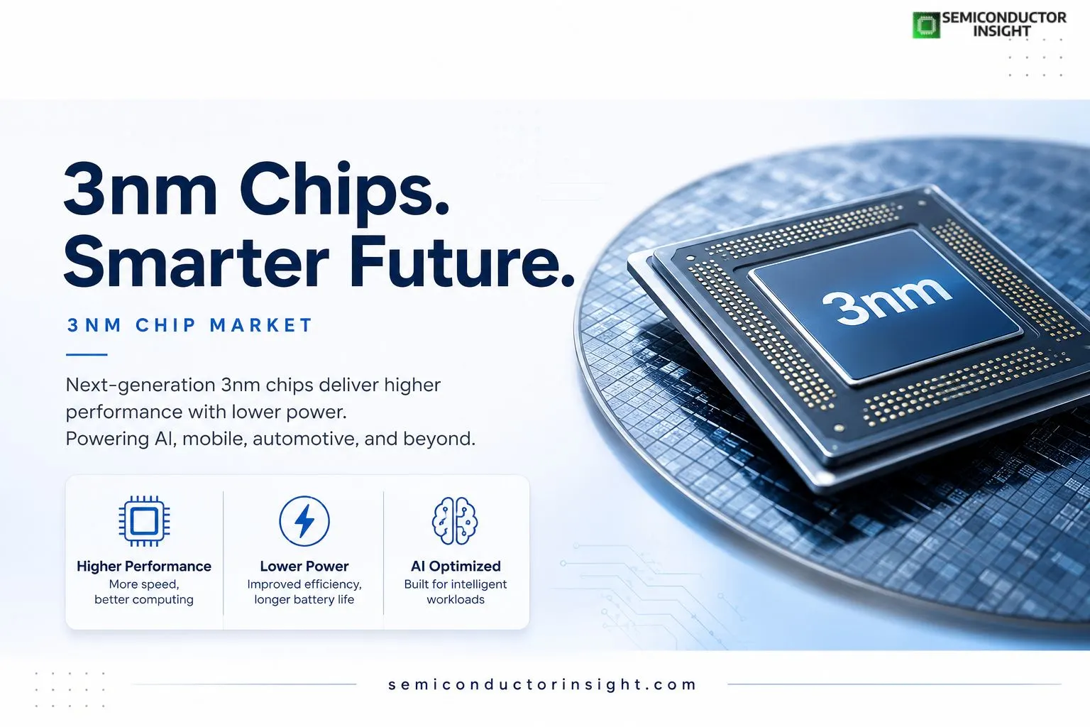
Why Leading Tech Giants Are Betting Billions on 3nm Nodes Right Now?
The semiconductor landscape continues evolving at a rapid pace, with manufacturers pushing physical limits to deliver chips that balance unprecedented performance, energy savings, and compact designs.
As demand surges for artificial intelligence applications, advanced smartphones, and efficient servers, the 3nm node stands out as a pivotal advancement in this ongoing race.
For instance, in February 2026; Renesas Electronics has announced a new ternary content addressable memory (TCAM) technology based on a 3nm FinFET process. At the International Solid-State Circuits Conference (ISSCC 2026) in San Francisco, the company showed the development, which delivers higher memory density, lower power consumption and improved functional safety for next-generation automotive and data-intensive systems.
What Is 3nm Technology?
At its core, 3nm technology refers to the latest commercial generation of semiconductor manufacturing processes following the 5nm node. Unlike literal measurements of every feature on the chip, the ‘3nm’ label serves primarily as an industry marketing designation that highlights significant improvements in transistor density, speed, and power efficiency compared to prior generations.
TSMC employs an enhanced FinFET transistor structure for its N3 process, achieving roughly 33 percent higher transistor density than its 5nm counterpart, along with 25-30 percent lower power consumption at the same performance level or 10-15 percent higher speed at equivalent power. Samsung took a bolder step by introducing Gate-All-Around (GAA) transistors, branded as MBCFET with nanosheet channels, in its initial 3nm production starting mid-2022. This architecture wraps the gate around the channel on all sides for better control, enabling up to 45 percent power reduction, 23 percent performance gain, and 16 percent smaller area versus its 5nm process.
Intel pursues its own ‘Intel 3’ node, which refines FinFET designs with extreme ultraviolet lithography enhancements rather than adopting the exact 3nm nomenclature. These variations underscore how each foundry tailors the node to specific customer needs while delivering generational leaps in capability. The technology relies heavily on multipatterning techniques with EUV lithography to create the intricate patterns required at this scale.
Inside the Race for Volume Production and Real-World Deployments
- TSMC achieved volume production of its 3nm process by late 2022, with strong yields reported during the ramp-up at facilities like Fab 18. Apple became an early and major adopter, securing substantial capacity for chips powering iPhone models and M-series processors in Macs. Reports indicate TSMC scaled monthly wafer output significantly, supporting hundreds of thousands of advanced processors annually in the initial phases.
- Samsung began initial 3nm production in June 2022 using its GAA technology. One notable early application appeared in cryptocurrency mining ASICs from MicroBT, such as the Whatsminer M56S++, demonstrating the process’s viability for high-performance, power-sensitive workloads. Qualcomm also reserved capacity on Samsung’s node for potential mobile and computing chips.
- These deployments highlight how 3nm chips enable longer battery life in portable devices while handling intensive AI tasks in data centers. For instance, enhanced efficiency directly supports the proliferation of edge AI features in consumer electronics and more sustainable server operations globally.
Navigating Geopolitical Shifts and Manufacturing Expansions
Government initiatives worldwide influence the 3nm ecosystem. The US CHIPS Act has spurred investments in domestic advanced manufacturing, with TSMC establishing fabs in Arizona that include plans for 3nm FinFET technologies in subsequent phases. This diversification aims to bolster supply chain resilience amid growing concerns over concentration in Asia.
Taiwan remains central, where TSMC’s facilities produce the majority of leading-edge nodes. Events like the 2024 earthquake temporarily affected output, underscoring vulnerabilities, yet rapid recovery efforts and ongoing capacity expansions demonstrate the industry’s robustness. Samsung continues scaling its South Korean and other global sites, while broader international collaborations seek to distribute expertise in extreme ultraviolet tools and materials science critical for sub-5nm nodes.
You Can Go Through Our Latest Updated Insights Here: https://semiconductorinsight.com/report/3nm-chip-market/
Emerging Applications Fuelling Demand in AI and Beyond
- The 3nm node excels in applications requiring dense integration and low power draw.
- Smartphone processors benefit from faster neural engines for on-device machine learning, while high-performance computing chips tackle complex simulations and training workloads more efficiently.
- Automotive systems increasingly incorporate these advanced nodes for autonomous driving capabilities, and networking equipment leverages them for higher bandwidth with reduced energy footprints.
- MediaTek developed its first 3nm chip with TSMC, targeting volume production around 2024 for various consumer devices. Xiaomi introduced a 3nm-based XRING O1 processor in its premium phones and tablets by 2025, showcasing broader ecosystem adoption.
- These examples illustrate the technology’s transition from flagship exclusivity to wider accessibility.
Technical Challenges and Engineering Triumphs at the Frontier
Fabricating at 3nm involves overcoming quantum effects and heat management hurdles. Foundries invest heavily in new materials, precise deposition techniques, and design tools that optimize for GAA structures or refined FinFETs. Yields have improved progressively, allowing cost-effective scaling despite the immense complexity billions of transistors packed into areas smaller than a square millimeter.
Ongoing refinements target even better power-performance-area metrics in subsequent iterations, such as Samsung’s second-generation 3nm goals aiming for up to 50 percent power savings. Collaboration between equipment suppliers, material providers, and chip designers proves essential to sustaining progress.
Global Collaboration Driving the Next Wave of Innovation
- Partnerships across borders accelerate 3nm advancements.
- Universities and research institutions contribute foundational work on nanosheet transistors and lithography, while companies share knowledge on process integration.
- This collective effort ensures the semiconductor industry meets exploding computational demands from AI, 5G/6G infrastructure, and scientific computing.
As production volumes grow into the hundreds of thousands of wafers monthly across key players, the 3nm era solidifies its role in shaping technology for years ahead. Engineers and strategists alike monitor how these chips influence everything from personal gadgets to large-scale data infrastructure, marking a significant chapter in the relentless pursuit of smaller, smarter electronics.

Comments (0)