Key Statistics
Key Takeaways
- Logic devices lead the product mix with 42% share because flagship mobile processors, AI accelerators and high-performance computing silicon capture the greatest economic value from advanced-node performance, power and density gains.
- Smartphones remain the leading application, while data centers are the strongest strategic growth area as AI and cloud processors shift toward 3nm-class technology to improve compute performance per watt.
- Asia Pacific dominates advanced-node manufacturing with more than 60% of global semiconductor production capacity in the current market structure, led by Taiwan and South Korea.
- TSMC and Samsung are the core commercial 3nm foundries. TSMC’s N3 family represented 24% of its wafer revenue in 2025 and 25% in 1Q 2026, while Samsung’s SF3 uses gate-all-around nanosheet transistors.
- The 3nm family is broadening rather than standing still. TSMC N3E and N3P are in volume production, N3X entered volume production in 2025, and N3C is scheduled for volume production in 2026.
3nm Chip Market Overview
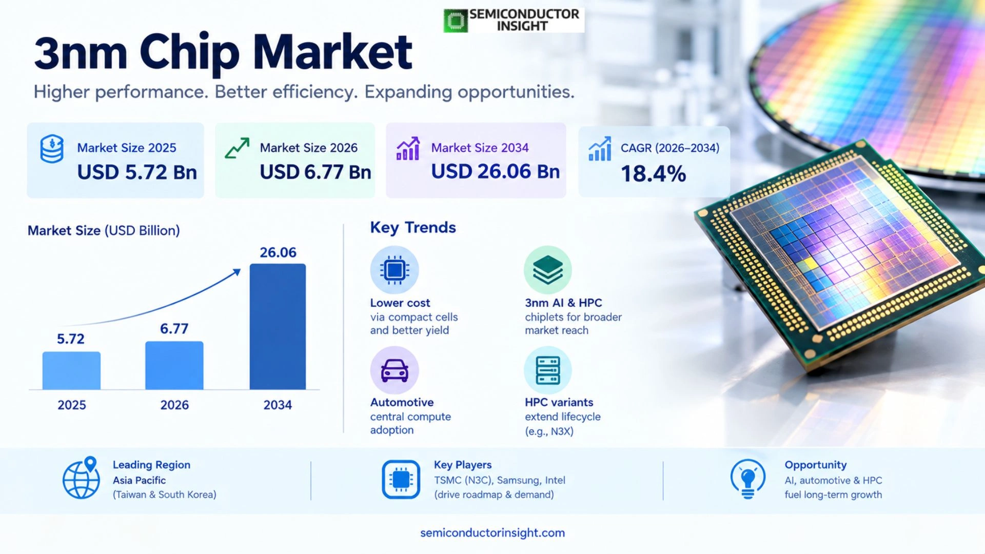
3nm Chip market is valued at USD 5.72 billion in 2025 and is projected to reach USD 26.06 billion by 2034, representing an 18.4% CAGR during 2026–2034. The 2026 estimated market size is USD 6.77 billion. Asia Pacific is the dominant manufacturing region through Taiwan and South Korea, where the two major commercial 3nm foundry ecosystems are concentrated.
3nm is a foundry process-node generation rather than a literal measurement of one physical transistor dimension. The node combines aggressive lithographic scaling, advanced device structures, tighter design rules and extensive design-technology co-optimization to improve logic density and energy efficiency. TSMC’s 3nm family uses FinFET technology across N3 variants, while Samsung introduced gate-all-around nanosheet transistors at 3nm through its MBCFET architecture.
The addressable market includes chips fabricated on 3nm-class processes rather than one single product category. Flagship smartphone application processors were among the earliest high-volume adopters, followed by high-performance computing and AI designs. As foundry yield and ecosystem maturity improve, more customers can use 3nm for CPUs, GPUs, custom accelerators and communications silicon without absorbing the cost and risk of first-generation production.
Economics are shaped by wafer cost, design cost and the value of power efficiency. Advanced masks, EUV lithography and large engineering teams make 3nm expensive, so the node is most attractive when customers can monetize performance, battery life, compute density or reduced energy consumption. Chiplets and advanced packaging also help customers use 3nm only for compute-critical dies while keeping I/O, analog or other functions on less expensive nodes.
Segment Analysis: By Type
By type, the market covers Memory, Logic Devices, Microprocessors, Analog Devices and Others. Logic devices hold the leading position with 42% share because advanced-node foundry capacity is concentrated on high-value mobile and compute products where power, performance and area improvements justify the cost of 3nm design and manufacturing.
| Type | 3nm role | Market position |
|---|---|---|
| Logic Device | Logic includes application processors, custom ASICs, connectivity and digital functions that benefit directly from higher transistor density and lower switching power. Large logic blocks can use advanced standard cells, SRAM and high-speed interfaces tailored for mobile or HPC use. | Largest type with 42% share. Demand is driven by flagship mobile, cloud, AI and advanced digital systems where power efficiency and transistor density have high economic value. |
| Microprocessor | CPUs and GPUs use 3nm to increase compute density and performance per watt. High-end PC, server and AI processors can combine 3nm compute tiles with I/O or cache built on other nodes through chiplet packaging. | A high-value growth segment. Data-center energy constraints and increasing accelerator complexity make advanced-node efficiency commercially important even when wafer and design costs are high. |
| Memory | The memory category includes selected advanced SRAM and memory-related logic as well as future DRAM and NAND-related functions that may adopt leading nodes where density and peripheral logic justify the transition. | A smaller direct 3nm market than logic because core DRAM and NAND cell scaling follows specialized process roadmaps, but memory controllers and cache-rich compute products increase advanced-node content. |
| Analog Devices | Analog functions do not scale as efficiently as digital logic, and high-voltage devices often prefer mature nodes. Selected mixed-signal blocks can still be integrated into 3nm SoCs to reduce interfaces and package count. | A niche within the 3nm market. Customers generally reserve the most advanced process for digital functions and use chiplets or companion dies for analog and power functions. |
Process architecture and customer-model segmentation
The commercial 3nm landscape is differentiated by transistor architecture, process variant and customer business model. TSMC uses an extensive N3 FinFET family with variants optimized for mobile, HPC, density and cost. Samsung introduced gate-all-around nanosheet technology at 3nm. Fabless customers rely on foundry process design kits and IP, while integrated device manufacturers can coordinate process, design and packaging internally.
| Axis | Segments | Commercial implication |
|---|---|---|
| By Process Architecture | FinFET 3nm · Gate-All-Around 3nm · Optimized 3nm Variants | TSMC’s N3 family extends FinFET scaling through N3E, N3P, N3X and N3C, while Samsung’s SF3 uses GAA nanosheets. The architecture affects drive current, leakage, standard-cell density, SRAM behavior and design methodology. |
| By Customer Model | Fabless Semiconductor Companies · Integrated Device Manufacturers · Captive Product Companies | Fabless firms buy foundry wafers and rely on external process ecosystems; IDMs can co-optimize their own process and products; captive product companies use leading nodes to differentiate devices, services and system performance. |
Segment Analysis: By Application
By application, Smartphones lead the current market, followed by computers, data centers, automotive electronics and other advanced systems. Smartphones created early production scale, while AI and data-center chips are becoming the most important source of incremental wafer value because power efficiency can reduce operating cost across very large compute fleets.
| Application | Demand characteristics |
|---|---|
| Smartphones | Flagship mobile processors need high CPU, GPU, AI and imaging performance within strict battery and thermal limits. 3nm enables more transistors at a given die area and can reduce active power, supporting richer on-device AI and graphics without increasing handset cooling capacity. |
| Data Centers | AI accelerators, server CPUs and custom cloud ASICs value 3nm for performance per watt. Data-center operators pay not only for silicon but also electricity, cooling and rack density, so a more expensive advanced-node processor can be attractive if it improves usable compute within a fixed power envelope. |
| Computers | Premium notebooks, desktops and workstations use 3nm-class processors to improve single-thread performance, integrated graphics and battery life. Chiplet architectures allow designers to place compute tiles on 3nm while using mature nodes for I/O and other functions. |
| Automotive Electronics | Central compute and autonomous-driving systems require increasing AI, graphics and sensor-processing capability. Automotive adoption trails smartphones because qualification and cost are demanding, but premium software-defined vehicles create a long-term path to advanced-node processors. |
| Others | Telecommunications, networking, edge AI and specialized accelerators use 3nm when bandwidth, power or integration justify the cost. Many products adopt advanced nodes selectively through compute chiplets rather than migrating every function. |
Regional Analysis
Asia Pacific dominates the 3nm Chip market with more than 60% of global semiconductor production capacity in the current market structure. Taiwan and South Korea are the primary commercial 3nm manufacturing centers through TSMC and Samsung. North America is a major design and demand hub, while Europe contributes critical lithography, semiconductor equipment and advanced-compute customers.
How does the 3nm ecosystem differ across regions?
Advanced-node manufacturing and advanced-node consumption are geographically different. Asia Pacific carries most commercial 3nm wafer production, North America hosts many leading fabless customers and hyperscalers, and Europe supplies indispensable lithography and equipment technology. Japan is rebuilding advanced semiconductor capability while China invests heavily in domestic semiconductor manufacturing but faces tighter access to leading-edge lithography technology.
| Region | Market position | Growth outlook | Demand profile | What decides supplier selection |
|---|---|---|---|---|
| Asia Pacific | Dominant manufacturing region | Very high | Foundry, mobile & HPC | Yield, EUV capacity and customer ecosystem |
| North America | Design / demand hub | Very high | AI, cloud & premium compute | Foundry access, packaging and IP ecosystem |
| Europe | Critical equipment / specialty hub | High | Lithography, auto & HPC | Equipment leadership and design collaboration |
| South America | Small downstream market | Selective | Cloud & premium devices | Imported advanced silicon |
| Middle East & Africa | Emerging demand | High from small base | AI data centers & sovereign compute | Access to leading processors and supply |
Competitive Landscape
The commercial 3nm foundry market is led by TSMC and Samsung. The broader competitive set also includes Intel Foundry Services as an advanced-node competitor, GlobalFoundries as a specialty foundry participant and SMIC as China’s leading domestic foundry. TSMC and Samsung collectively account for the overwhelming majority of commercial 3nm production in the current market structure.
TSMC has the broadest 3nm product family and the strongest demonstrated production scale. N3 entered volume production in 2022, N3E expanded the family for mobile and HPC, N3P adds further performance and density improvement, N3X targets extreme HPC performance and entered volume production in 2025, and N3C focuses on compact cells and cost-effective migration with volume production expected in 2026.
Samsung differentiates with gate-all-around transistor architecture at 3nm. Its MBCFET implementation uses nanosheet channels and allows design flexibility through channel-width tuning. Samsung states that its first-generation 3nm process can reduce power by up to 45%, improve performance by 23% and reduce area by 16% compared with its 5nm process under defined conditions.
Intel competes primarily through 20A and 18A rather than a process named 3nm, showing why node labels are not directly comparable across foundries. GlobalFoundries focuses on specialty technologies rather than commercial 3nm production, while SMIC’s role is shaped by domestic demand and equipment-access constraints. Foundry competition increasingly depends on packaging, IP, EDA enablement and manufacturing yield as much as nominal node name.
Competitive tier structure
| Tier | Companies | Basis of competition |
|---|---|---|
| Commercial 3nm leaders | TSMC; Samsung Foundry | Volume manufacturing, EUV capacity, mobile/HPC customer base, process variants and advanced packaging |
| Advanced-node competitor | Intel Foundry Services | 18A/20A roadmap, U.S. manufacturing, advanced packaging and external-foundry ambitions |
| Specialty / emerging foundries | GlobalFoundries; SMIC | Specialty-node focus or domestic advanced-node development rather than current large-scale 3nm production |
Key companies profiled in the report scope
- Taiwan Semiconductor Manufacturing Company (TSMC)
- Samsung Foundry
- Intel Foundry Services
- GlobalFoundries
- Semiconductor Manufacturing International Corporation (SMIC)
3nm Production Capacity & Yield Analysis
3nm capacity is determined by EUV tool availability, cleanroom space, process-step throughput, wafer yield and advanced-packaging capacity. Nominal wafer-start capacity does not directly equal sellable chip output because large dies and early process versions can have lower yield. Mature 3nm variants become economically more valuable as defect density falls and customers can reuse proven IP.
TSMC’s revenue mix provides a useful indication of production scale. The company reported that 3nm represented 24% of total wafer revenue in 2025 and 25% in the first quarter of 2026. This reflects broad commercial use across smartphone and HPC customers rather than a small pilot market. Revenue share can remain high even as 2nm begins ramping because mature 3nm designs continue in volume for several product generations.
Foundry capacity also depends on design enablement. Customers need standard cells, SRAM, high-speed interfaces, chip-package co-design and verified EDA flows. A process with good transistor performance but limited IP cannot convert wafer capacity into customer tape-outs. TSMC’s N3 variants emphasize backward-compatible design rules, while Samsung uses its SAFE ecosystem to improve design readiness.
Market Dynamics
Growth is driven by AI accelerators, flagship smartphones, high-performance computing, energy-efficiency requirements and wider 3nm foundry maturity. Restraints include high wafer and design cost, EUV capacity, yield learning and rapid migration toward 2nm. Opportunities center on N3 derivatives, AI chiplets, advanced packaging, automotive compute and mature 3nm cost optimization.
MARKET DRIVERS
Drivers Impact Analysis*
| Factor | Forecast impact* | Geographic relevance | Impact timeline |
|---|---|---|---|
| AI / HPC compute demand | High | North America, Asia Pacific | Short to long term |
| Flagship smartphone processors | High | Global | Persistent |
| Energy efficiency requirements | High | Data centers & mobile | Persistent |
| Foundry process maturity | Medium to high | Taiwan, Korea | Medium term |
*Directional analytical rating; it is not a measured contribution to the headline CAGR.
AI rewards performance per watt
Training and inference processors require enormous compute throughput, but data-center power is constrained. Advanced nodes can deliver more transistors and higher frequency within a power envelope, making 3nm attractive for AI accelerators and custom cloud ASICs. The economic value is measured at rack and facility level rather than only at wafer cost.
Flagship mobile created the production base
High-end smartphones were early adopters because battery life and silicon area are highly valuable. Large mobile volumes helped foundries improve yield and broaden IP support. That production maturity lowers risk for later HPC and custom-ASIC customers.
3nm process variants expand addressable designs
One process optimization does not suit every customer. TSMC’s N3E, N3P, N3X and N3C variants target different combinations of performance, density, leakage and cost. A broader family allows customers to remain within one design ecosystem while selecting a better economic point for each product.
Chiplets make advanced nodes more economical
Designers can place compute-intensive logic on 3nm while leaving analog, I/O and other functions on mature nodes. This reduces expensive 3nm die area and can improve yield. Advanced packaging therefore increases the number of systems that can benefit from 3nm without moving the entire chip onto the node.
MARKET RESTRAINTS
Restraints Impact Analysis*
| Factor | Forecast impact* | Geographic relevance | Impact timeline |
|---|---|---|---|
| High wafer and mask cost | High | Global customers | Persistent |
| Yield and design complexity | High | New process variants | Persistent |
| EUV equipment concentration | High | Foundry supply chain | Persistent |
| Migration toward 2nm | Medium to high | Leading-edge customers | Medium term |
*Directional analytical rating; it is not a measured contribution to the headline CAGR.
Design cost limits the customer base
3nm development requires expensive masks, IP, verification and engineering. Only products with high volume or high selling value can justify the investment. Smaller semiconductor companies often use mature nodes or buy platform chips instead of creating a custom 3nm design.
Yield matters more as die size increases
Large AI and server chips expose more wafer area to defects. Even with good defect density, a very large monolithic die can have lower yield than a smaller mobile processor. Chiplets mitigate this issue, but add packaging and system complexity.
EUV lithography is a concentrated dependency
Commercial 3nm production relies on EUV systems from a single equipment supplier and an extended network of optics, masks, photoresists and process-control tools. Capacity cannot be expanded instantly because equipment manufacturing and fab installation have long lead times.
2nm creates a moving technology frontier
The most performance-sensitive customers migrate quickly. TSMC started 2nm high-volume manufacturing in late 2025, while Samsung is also advancing GAA nodes below 3nm. This can shift premium new designs away from 3nm, although the older node can continue growing in absolute volume as it becomes more mature and cost effective.
MARKET OPPORTUNITIES
Use N3C and mature N3 variants to lower cost
As the 3nm ecosystem matures, compact cells, better yield and simpler process options can reduce effective cost. TSMC N3C targets cost-effective scaling and IP reuse, creating a pathway for customers that could not justify the earliest N3 variants.
Expand 3nm AI and HPC chiplets
AI systems benefit from using 3nm only where compute density matters most. Chiplet architectures can combine 3nm compute tiles with memory, I/O and analog dies from other nodes, widening the commercial market without forcing every function onto the most expensive process.
Move into automotive central compute
High-end software-defined vehicles require more AI and graphics performance. Once 3nm has several years of production maturity, automotive customers can adopt the node for central processors where performance and energy efficiency justify long qualification cycles.
Extend lifecycle through differentiated HPC variants
N3X targets high-performance computing with higher speed and improved power efficiency. Specialized variants can keep the 3nm family relevant after mainstream mobile begins moving to 2nm by serving products that value mature yield and established design ecosystems.
3nm Chip Value Chain Analysis
Design enablement starts years before wafer production
3nm customers need mature EDA tools, IP blocks and design rules before tape-out. SRAM, SerDes and standard-cell behavior can determine practical chip density as much as transistor scaling. Foundries work with ecosystem partners so customer designs converge on timing, power and manufacturability.
EUV fabrication is capital and process intensive
A 3nm wafer passes through repeated lithography, deposition, etch, clean and metrology steps. EUV reduces some multi-patterning complexity but introduces its own mask, resist and stochastic-defect challenges. Stable high-volume production requires extremely tight process control across thousands of wafers.
Packaging determines system-level benefit
Large AI devices increasingly use advanced 2.5D or 3D packaging to combine 3nm compute with HBM and I/O dies. Package power delivery, thermal design and interconnect bandwidth can determine whether the transistor-level gains are realized at system scale.
End markets monetize 3nm differently
Smartphones monetize battery life and features, while data centers value compute per watt and rack density. PCs value performance and efficiency, and automotive systems value consolidated compute. These differences determine which process variant, die size and packaging architecture is economically optimal.
Recent Developments in the 3nm Chip Market
TSMC 3nm reaches 25% of quarterly wafer revenue
TSMC reported that 3nm technology contributed 25% of wafer revenue in the first quarter of 2026, demonstrating continued high-volume adoption as the company simultaneously ramps newer 2nm technology.
TSMC prepares N3C volume production
TSMC’s 2025 annual report states that N3C received customer tape-out in 2025 and is expected to enter volume production in 2026. N3C uses compact cells, simplified processing and backward-compatible design rules to improve cost effectiveness and IP reuse.
TSMC N3X enters volume production
TSMC reported that its N3X technology, tailored for high-performance computing, started volume production in 2025 after qualification in 2024. The variant extends the 3nm family toward higher-performance applications.
TSMC 3nm accounts for 24% of annual wafer revenue
In its third full year of volume ramp, TSMC’s 3nm technologies represented 24% of total wafer revenue, supported by smartphone and high-performance computing demand.
Samsung continues SF3 gate-all-around production
Samsung Foundry’s current logic-node portfolio lists SF3 in mass production using gate-all-around nanosheet technology, extending its differentiated 3nm architecture across advanced computing applications.
REPORT SCOPE & SEGMENTATION
| Attribute | Details |
|---|---|
| Study Period | 2020–2034 |
| Base Year | 2025 |
| Estimated Year | 2026 |
| Forecast Period | 2026–2034 |
| Historical Period | 2020–2025 |
| Market Size 2025 | USD 5.72 billion |
| Market Size 2034 | USD 26.06 billion |
| Growth Rate | CAGR of 18.4% from 2026–2034 |
| Unit | Value (USD Million/Billion) and chip/wafer output where applicable |
| Segmentation | By Type, By Application, By End User, By Process Architecture, By Customer Model, By Region |
| By Type | Memory · Logic Device · Microprocessor · Analog Devices · Others |
| By Application | Smartphones · Computers · Data Centers · Automotive Electronics · Others |
| By End User | Consumer Electronics · Enterprise IT · Automotive · Telecommunications · Others |
| By Process Architecture | FinFET 3nm · Gate-All-Around 3nm · Optimized 3nm Variants |
| By Customer Model | Fabless Semiconductor Companies · Integrated Device Manufacturers · Captive Product Companies |
| By Region | Each region analysed by chip type, application, end user, process architecture, customer model and country ecosystemNorth AmericaUnited States, Canada, MexicoEuropeNetherlands, Germany, France, Belgium and other European marketsAsia PacificTaiwan, South Korea, Japan, China, Singapore and other Asian marketsSouth AmericaBrazil, Argentina and other South American marketsMiddle East & AfricaSaudi Arabia, UAE, Israel, South Africa and other MEA markets |
| Key Companies Profiled | Taiwan Semiconductor Manufacturing Company (TSMC) · Samsung Foundry · Intel Foundry Services · GlobalFoundries · Semiconductor Manufacturing International Corporation (SMIC) |
| Customization Scope | Free report customization equivalent to up to four analyst working days with purchase. Addition or alteration to country, regional and segment scope. |
Frequently Asked Questions
What is the 2025 size of the 3nm Chip market?
The market is valued at USD 5.72 billion in 2025 and is projected to reach USD 26.06 billion by 2034. The 2026 estimate is USD 6.77 billion and the 2026–2034 CAGR is 18.4%, reflecting continued expansion across flagship mobile, AI and high-performance computing.
Which 3nm chip type leads the market?
Logic devices lead with 42% share because high-value digital products capture the greatest benefit from transistor density and power efficiency. Application processors, custom ASICs and advanced compute logic can justify the high wafer and design cost more readily than many analog or mature-node functions.
Which application leads 3nm demand?
Smartphones remain the leading application because flagship mobile processors were among the first high-volume 3nm products. Data centers are a major growth opportunity as AI accelerators and server processors increasingly value compute performance per watt and advanced chiplet integration.
Which region leads 3nm production?
Asia Pacific dominates with more than 60% of global semiconductor production capacity in the current market structure. Taiwan and South Korea are the key 3nm production centers through TSMC and Samsung, while Japan supplies critical materials and equipment.
What is the estimated market size in 2026?
The 2026 market size is USD 6.77 billion. Growth is supported by continued smartphone volume, AI and HPC tape-outs, mature foundry yield and expansion of process variants such as N3P, N3X and N3C.
What is the difference between TSMC and Samsung 3nm?
TSMC’s N3 family uses FinFET transistor technology across several optimized process variants. Samsung introduced gate-all-around nanosheet MBCFET architecture at 3nm. The two foundries therefore use different transistor structures, design rules, IP ecosystems and performance trade-offs despite sharing the 3nm marketing label.
Why is 3nm expensive?
The node requires extensive EUV lithography, advanced masks, large design teams, complex verification and premium wafer processing. Foundry wafer prices are only part of total cost; IP licensing, packaging and mask sets can also be substantial. High-volume or high-value products are best positioned to absorb the investment.
How does chiplet design expand 3nm adoption?
Chiplets allow customers to use 3nm only for compute-intensive logic while keeping I/O, analog or other functions on cheaper nodes. This reduces expensive 3nm die area, can improve yield and lets system designers combine several optimized technologies in one advanced package.
Will 2nm replace 3nm immediately?
No. Leading customers migrate first, but mature 3nm technology can continue growing through better yield, lower effective cost and established IP. TSMC’s expanding N3 family shows how an advanced node can remain commercially important for years even after a newer node starts production.
What does the report cover?
The report covers memory, logic, microprocessor and analog 3nm chips; smartphone, computer, data-center and automotive applications; consumer, enterprise, automotive and telecom end users; process architectures and customer models; five global regions; production and yield analysis; and the profiled foundry companies.
Research Sources & Evidence Base
View primary and authoritative evidence used in this overview
- TSMC. 2025 Annual Report – Primary evidence on N3 annual wafer-revenue share, N3E/N3P production, N3C tape-out and 2026 production plan, and N3X volume production.
- TSMC. 1Q 2026 Investor Presentation – Primary evidence that 3nm represented 25% of TSMC wafer revenue in 1Q 2026.
- TSMC. HPC Advanced Technologies – N3 Family – Official technical information on N3P and N3X positioning and production.
- Samsung Foundry. Logic Node – SF3 – Official current process portfolio showing 3nm GAA SF3 in mass production.
- Samsung Electronics. 3nm Production Using GAA Architecture – Primary technical evidence on MBCFET GAA architecture and 3nm power, performance and area positioning.
Get Sample Report PDF for Exclusive Insights
Report Sample Includes
- Table of Contents
- List of Tables & Figures
- Charts, Research Methodology, and more...
 Download Sample Report PDF