
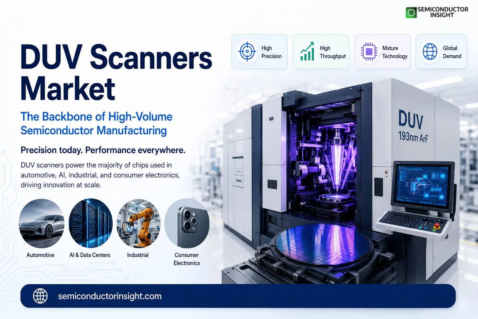
Why DUV Scanners Remain the Backbone of Modern Semiconductor Manufacturing
Although Extreme Ultraviolet (EUV) lithography receives much of the industry’s attention, Deep Ultraviolet (DUV) scanners continue to manufacture the overwhelming majority of semiconductor devices produced worldwide. From automotive microcontrollers and power management ICs to memory chips, image sensors, RF devices, and industrial processors, DUV systems remain indispensable for high-volume fabrication.
Operating primarily with 193 nm ArF and 248 nm KrF laser wavelengths, these scanners pattern billions of microscopic transistor structures with nanometer-scale precision. As more than 100 semiconductor fabrication facilities are planned, under construction, or expanding globally, DUV scanners remain one of the most actively deployed equipment categories supporting mature and advanced process technologies.
Beyond Smartphones Where DUV Scanners Quietly Shape Everyday Electronics
- The influence of DUV scanners extends far beyond premium processors.
- Automotive electronic control units, medical imaging systems, industrial automation controllers, consumer appliances, networking hardware, and renewable energy converters all rely on chips fabricated using DUV lithography.
- Even many AI servers incorporate supporting components manufactured through mature process nodes using DUV exposure.
- Recent semiconductor investments by TSMC, Samsung Electronics, Intel, GlobalFoundries, SMIC, and Texas Instruments continue expanding production capacity for chips manufactured on technology nodes ranging from 180 nm to 28 nm, where DUV remains the primary lithography platform.
Manufacturing Scale Shows Why DUV Remains Indispensable
Modern semiconductor manufacturing demonstrates the remarkable scale at which DUV scanners operate. Global semiconductor production now exceeds 1 trillion integrated circuits annually, while more than 200 million silicon wafers are processed every year across 200 mm and 300 mm fabrication facilities. A single advanced DUV scanner can expose well over 250 wafers per hour, depending on the lithography configuration and process node.
Today’s semiconductor fabs often operate continuously, processing thousands of wafers each day to satisfy growing demand from automotive electronics, artificial intelligence infrastructure, industrial automation, and consumer technology. These production volumes highlight why DUV systems remain fundamental to the semiconductor supply chain despite the gradual adoption of EUV technology for the most advanced logic chips.
The Precision behind Every Exposure Layer
Producing modern semiconductor devices requires extraordinary optical precision. During fabrication, DUV scanners project circuit patterns from photomasks through sophisticated projection optics onto photoresist-coated silicon wafers. Advanced positioning systems capable of nanometer-scale accuracy ensure every exposure aligns perfectly with previously patterned layers.
Multiple-patterning techniques including double and quadruple patterning allow DUV scanners to manufacture structures significantly smaller than the exposure wavelength itself. These engineering innovations have enabled continued scaling while extending the practical lifespan of existing lithography platforms across multiple semiconductor generations.
For More Detailed Insights, You Can Surf Our Latest Report Here: https://semiconductorinsight.com/report/duv-scanners-market/
Lithography Workflow
Integrated Circuit Design
│
▼
Photomask Fabrication
│
▼
Photoresist Coating
│
▼
DUV Exposure
│
▼
Pattern Development
│
▼
Etching and Deposition
│
▼
Multi-Layer Chip Manufacturing
Artificial Intelligence Is Increasing Demand beyond Leading Edge Chips
The rapid expansion of artificial intelligence infrastructure has increased demand not only for advanced processors but also for numerous supporting semiconductor devices manufactured using DUV lithography.
AI servers require networking controllers, memory management circuits, voltage regulators, optical communication chips, storage controllers, and sensor interfaces that frequently utilize mature manufacturing technologies. The continuing construction of hyperscale data centers and AI computing clusters therefore strengthens utilization of DUV-based fabrication lines alongside leading-edge EUV production.
Equipment Intelligence Is Becoming as Important as Optical Performance
- The newest generation of DUV scanners integrates artificial intelligence, predictive maintenance software, machine learning algorithms, and real-time process monitoring to maximize productivity. Thousands of sensors continuously monitor vibration, thermal stability, stage positioning, optical alignment, laser consistency, and environmental conditions.
- Predictive analytics enables maintenance teams to identify potential issues before production interruptions occur, reducing downtime and improving wafer throughput. Digital twins and remote diagnostics are increasingly supporting global semiconductor manufacturers as fabrication facilities become larger, more automated, and highly interconnected.
Recent Industry Developments Reflect Continuing Investment
Recent global semiconductor initiatives continue reinforcing the strategic importance of DUV lithography. The United States has expanded domestic fabrication through the CHIPS and Science Act, while Europe advances production under the European Chips Act.
Japan has accelerated investments in advanced manufacturing partnerships, and India has launched new semiconductor fabrication projects aimed at strengthening domestic electronics production. At the same time, established manufacturers continue expanding mature-node capacity to support electric vehicles, industrial robotics, telecommunications infrastructure, and medical electronics, all of which depend extensively on DUV-based manufacturing.
A Technology That Continues Powering Semiconductor Innovation
While EUV represents the newest chapter in lithography evolution, DUV scanners remain the production backbone of the semiconductor industry. Their versatility, productivity, precision, and compatibility with a wide range of process technologies ensure they continue enabling billions of chips that power modern transportation, communication, healthcare, industrial automation, artificial intelligence, and consumer electronics.
Rather than being replaced, DUV lithography continues evolving through smarter software, higher throughput, improved overlay accuracy, and advanced patterning techniques, making it one of the most enduring technologies in semiconductor manufacturing.

Comments (0)