

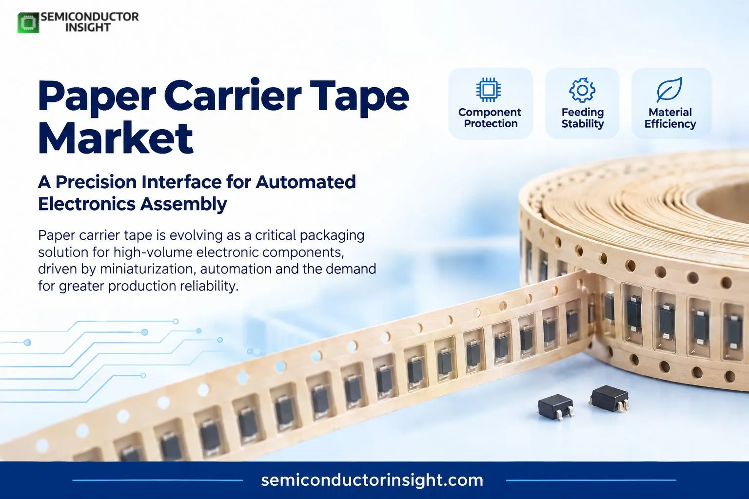
Why Component Miniaturization Is Rewriting Specifications in paper carrier tape market?
A semiconductor factory can spend millions on equipment and process control, yet the final movement of a tiny electronic component can still depend on a deceptively simple strip of packaging. Paper carrier tape is used to hold and transport electronic components in precisely formed pockets before automated placement. Its importance becomes clearer as components shrink, production speeds rise and assembly lines demand consistent feeding.
DNP, which has supplied cover-tape solutions for paper carriers for more than 20 years, identifies paper carrier tape applications covering MLCCs, inductors, piezoelectric elements and varistors. Its top tapes are engineered to maintain stable surface characteristics under temperature and humidity exposure, helping reduce sticking and component ejection during assembly.
A tiny package carrying a much larger manufacturing responsibility
Paper carrier tape is not simply a strip used to organize components. The tape has to maintain pocket geometry, component orientation and feeding stability while moving through automated equipment. The cover tape then seals the pockets without creating excessive peel force or releasing static charges that could interfere with sensitive components.
The basic movement can be visualized as:
Component production → Pocket forming → Component loading → Top-tape sealing → Reel winding → Transportation → Feeder → Pick-and-place → PCB assembly
That chain explains why dimensional consistency matters. A minor pocket deformation can translate into feeding instability, component rotation or placement interruptions on a high-throughput SMT line.
Miniaturization is changing what “good packaging” means
- The electronics industry continues to push component footprints downward.
- 3M notes that shrinking electronic components are creating demand for carrier tapes with precise pocket designs because tilt, flipping and migration can interfere with automated pick-and-place operations.
- Its carrier-tape portfolio includes designs intended for different component geometries and ANSI/EIA dimensional requirements.
- Paper carrier tape therefore occupies an interesting position. It is particularly established for passive electronic components, where high-volume feeding and consistent pocket formation are essential.
- The emphasis is increasingly moving from simply holding a component to maintaining repeatable mechanical behavior throughout the entire automated feeding cycle.
The semiconductor backdrop is getting larger
The underlying semiconductor production ecosystem continues to expand in complexity. SEMI reported worldwide silicon wafer shipments of 12,973 million square inches in 2025, up 5.8% from the previous year. The organization linked renewed shipment growth to demand for advanced logic and high-bandwidth-memory-related applications driven by AI.
- At the manufacturing level, TSMC reported 15.0 million 12-inch-equivalent wafer shipments in 2025, compared with 12.9 million in 2024. It also manufactured 12,682 products for 534 customers, illustrating the enormous diversity of components flowing through the semiconductor ecosystem.
Paper carrier tape does not directly correspond to wafer shipments, but these figures demonstrate the scale and diversification of the electronics supply chain that ultimately feeds component packaging and assembly operations.
For additional report info, feel free to view our most recent edition: https://semiconductorinsight.com/report/paper-carrier-tape-market-size-share-trends-market/
ESD and humidity are now packaging specifications, not afterthoughts
- Electronic components can be vulnerable to electrostatic discharge and environmental exposure.
- This has pushed carrier-tape systems toward better control of surface resistivity, static behavior and dimensional stability.
- DNP specifically highlights the ability of its paper-carrier top tape to maintain surface resistivity and peel-charge characteristics after exposure to high temperature and humidity.
- That matters because uncontrolled electrostatic behavior can cause components to stick to packaging or jump out of pockets during feeding.
Pocket accuracy + ESD behavior + humidity resistance + controlled peel force = stable automated feeding
Sustainability is creating a second conversation around paper carriers
Paper-based packaging is receiving renewed attention as electronics manufacturers examine material efficiency and packaging waste. However, sustainability cannot come at the expense of dimensional accuracy. Carrier tape must still survive winding, transportation, storage and high-speed feeding.
This creates room for engineering improvements in paper structure, coatings, surface treatment and adhesive compatibility rather than a simple substitution of plastic with paper.
2026 manufacturing signals worth watching
The strongest development signals are emerging from the intersection of smaller components, automated assembly and precision packaging. Advanced packaging itself is also becoming more sophisticated. TSMC reported volume production of its 3nm SoIC stacking technology in 2025 and continued expanding CoWoS technologies for high-performance computing applications.
Although wafer-level advanced packaging and paper carrier tape serve different stages of the electronics chain, both reflect the same manufacturing direction: more functionality packed into smaller physical spaces.
Where the next specification changes may appear
Paper carrier tape market is likely to be shaped less by a single breakthrough and more by incremental engineering improvements. Manufacturers are working around tighter pocket tolerances, faster feeder operation, lower component movement, controlled electrostatic characteristics and better performance under changing humidity conditions.
The opportunity is especially relevant for high-volume passive-component assembly, where even a tiny packaging inconsistency can become a repeated production problem when multiplied across thousands or millions of placements.
In 2026, paper carrier tape is therefore best understood not as ordinary packaging, but as a precision interface between component manufacturing and automated electronics assembly. As semiconductor and electronics production become increasingly automated, the value of that interface lies in something simple but difficult to achieve consistently: making every tiny component arrive at exactly the right place, orientation and moment for the machine that will install it.

Comments (0)