
Why Advanced Chip Packaging Market is Redefining Semiconductor Efficiency?
Chip packaging market has evolved from a protective function into a strategic semiconductor innovation layer that directly influences performance, power efficiency, and device reliability. Traditionally, packaging simply safeguarded integrated circuits from environmental damage, but modern advancements have repositioned it as a core enabler of high-performance computing, artificial intelligence processors, automotive electronics, and advanced communication systems.
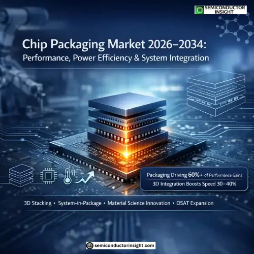
Industry estimates suggest that over 60% of semiconductor performance improvements in recent years are linked to packaging innovations rather than transistor scaling alone, demonstrating how packaging has become central to semiconductor competitiveness.
Today’s semiconductor ecosystem demands miniaturization, faster processing speeds, and lower energy consumption, pushing manufacturers toward advanced packaging technologies such as 3D stacking, wafer-level packaging, and system-in-package solutions. Companies like Taiwan Semiconductor Manufacturing Company, Intel Corporation, and Samsung Electronics are investing heavily in packaging innovation to address increasing chip complexity and rising global demand for computational power.
Key Highlights:
- For instance, in January 2026: The Taiwan Semiconductor Research Institute (TSRI) of the National Institutes of Applied Research (NIAR) officially unveiled the Chip-level Advanced Packaging Development Platform. This platform aims to propel Taiwan’s semiconductor industry from manufacturing leadership toward a new stage of system integration and application innovation leadership, securing a critical competitive advantage for the post-Moore era.
- For instance, in February 2026: Suchi Semicon, Gujarat’s pioneering Outsourced Semiconductor Assembly and Test (OSAT) Company, has declared the release of its new Power Packages (DPAK, TO-Series, IPAK) and QFN family (QFN, uQFN, DFN, XFN). The increasing need for small, dependable, and high-performing semiconductor packaging solutions is being addressed by these cutting-edge solutions for consumer electronics, automotive systems, electric vehicles (EVs), industrial applications, Internet of Things (IoT) devices, and renewable energy technologies.
- For instance, in January 2026: Paras Defence & Space Technologies established Paras Semiconductor to penetrate the semiconductor market in India. In order to fill India’s domestic capability gap, especially for defense requirements, the new subsidiary will set up an OSAT facility for sophisticated packaging and testing. By establishing a center for chiplet integration, this project seeks to improve performance, dependability, and control over vital technologies.
Technology Architecture Shaping the Modern Chip Packaging Landscape
3D Integration and Vertical Stacking Efficiency
One of the most influential developments is 3D chip packaging, where multiple semiconductor layers are stacked vertically to enhance processing capability while reducing footprint. This approach significantly improves data transfer speeds by nearly 30–40% while lowering energy consumption, making it essential for AI accelerators and data center processors.
The shift toward vertical integration also enables manufacturers to combine logic, memory, and sensors into a single compact unit, reducing latency and improving system performance.
System in Package Integration for Multifunction Devices
Another key advancement is system-in-package technology, which integrates multiple chips into a single module performing different functions. This approach supports the growing demand for wearable devices, IoT applications, and smart automotive systems where compactness and efficiency are critical.
System-in-package designs enable faster product development cycles and reduce board space requirements by nearly 50% in some applications, strengthening their commercial appeal.
Don’t Forget to Surf Our Updated Report for More Detailed Analysis:
https://semiconductorinsight.com/report/chip-packaging-market/
Material Science Innovation Powering Packaging Performance
Advanced chip packaging depends heavily on material engineering breakthroughs. Modern packaging incorporates organic substrates, ceramic materials, and advanced polymers to improve thermal conductivity and electrical performance.
For instance, high thermal conductivity materials help manage heat generated by high-density chips, preventing performance degradation. Semiconductor devices operating at high processing loads can experience temperature increases of over 20°C, making thermal management solutions essential for maintaining reliability.
Material innovation also enhances electromagnetic shielding and mechanical stability, which are critical for automotive and industrial electronics exposed to harsh environments.
Commercial Value and Strategic Benefits from Client Perspective
From a business standpoint, chip packaging delivers measurable operational and financial advantages. Improved performance density enables companies to develop more powerful products without increasing size, enhancing product differentiation in competitive markets.
Another major benefit is cost optimization. Advanced packaging allows integration of multiple components into a single unit, reducing assembly complexity and manufacturing steps. Companies adopting system-in-package technologies report production efficiency improvements of nearly 20%, lowering overall operational costs.
Packaging innovation also supports faster time-to-market, allowing manufacturers to quickly adapt to evolving consumer and enterprise technology demands. This agility is particularly valuable in sectors such as automotive electronics, cloud computing, and telecommunications infrastructure.
Operational Limitations and Business Challenges in Chip Packaging
Despite its advantages, advanced chip packaging introduces certain commercial and technical challenges. One significant concern is high initial investment requirements. Developing advanced packaging infrastructure demands substantial capital for equipment, materials, and skilled workforce training.
Another challenge is manufacturing complexity. Multi-layer chip structures require precise alignment and advanced testing procedures, increasing production risks and potential defect rates. Even minor packaging defects can reduce device reliability and increase failure rates in high-performance applications.
Supply chain constraints also present challenges, particularly for specialized substrates and materials. Fluctuations in material availability can impact production schedules and increase operational uncertainty for semiconductor manufacturers.
Testing Reliability and Quality Assurance Ecosystem
An essential aspect of the chip packaging market is testing and validation processes that ensure semiconductor reliability. Advanced inspection technologies, including automated optical inspection and thermal stress testing, verify package integrity before deployment.
Reliability testing helps reduce field failures and enhances product life cycles. Semiconductor manufacturers invest significantly in quality assurance, with testing processes accounting for nearly 15–20% of total packaging costs in high-performance chip production.
This focus on reliability is particularly critical in aerospace, medical electronics, and automotive sectors where performance failures can have severe consequences.
Chip packaging is no longer a secondary manufacturing step but a core differentiator shaping semiconductor value chains. Its influence spans performance optimization, system integration, cost efficiency, and product innovation across multiple industries.
For technology providers, investors, and enterprise clients, understanding packaging advancements provides insight into long-term semiconductor competitiveness and technological evolution. As electronic devices become more compact and powerful, chip packaging will remain central to enabling next-generation computing capabilities and commercial innovation.

Comments (0)