
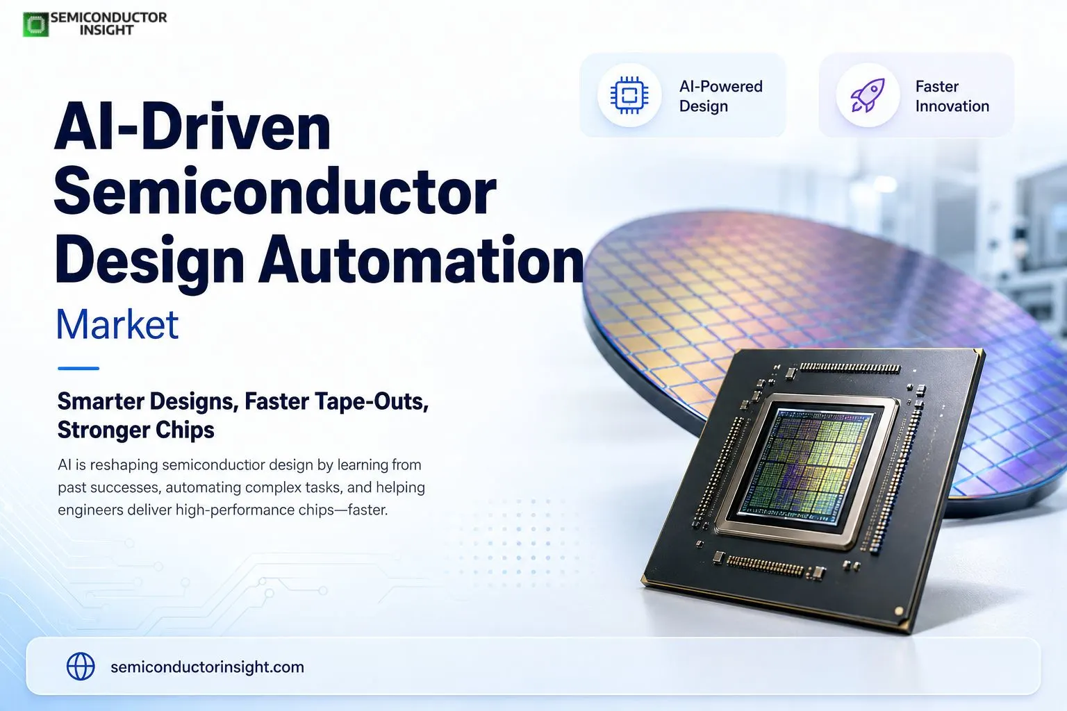
What Forward-Thinking Engineers See in the AI-Driven Semiconductor Design Automation Market Evolution?
Semiconductor design has always been a meticulous craft, balancing billions of transistors on tiny wafers while chasing better power efficiency and speed. Today, artificial intelligence steps into this intricate dance, turning what used to take months of manual iteration into smarter, faster processes that feel almost collaborative.
Engineers once spent endless hours tweaking layouts by hand. Now, AI systems analyse vast datasets from previous designs, suggesting optimizations that human teams might overlook after days of review. This shift feels less like automation and more like having a tireless partner who remembers every successful tape-out from the past decade.
From Concept to Certified Flow: Real Partnerships in Action
- Take the close work between TSMC and Cadence. Their expanded collaboration covers advanced nodes like N3, N2, and A16, delivering certified flows that handle everything from implementation to thermal analysis.
- These joint efforts produce silicon-proven IP blocks tailored for high-bandwidth memory and 3D-IC stacking, directly supporting the massive data movement needs of modern AI accelerators.
- Similar patterns appear with Synopsys tools integrated into foundry environments. Multi-agent workflows orchestrate tasks across the design lifecycle, moving from system architecture exploration all the way to manufacturing handoff.
- One documented outcome involves verification coverage jumping significantly while cutting regression times dramatically in complex SoC projects.
Learning from Past Designs: The Memory Effect in Tools
Machine learning techniques now appear at nearly every stage of the integrated circuit design flow, from high-level synthesis to final sign-off. Wikipedia’s overview of electronic design automation notes how these methods shorten turnaround times and improve power, performance, and area metrics.
Companies like MediaTek have shared experiences using tools such as Cadence Cerebrus, reporting noticeable reductions in die area and power consumption for their system-on-chip projects. These aren’t abstract lab experiments. They represent production designs reaching customers in consumer electronics and networking gear.
Government and Open Initiatives Fuelling Broader Access
Beyond commercial tools, public efforts play a key role. The OpenROAD project, supported through DARPA programs, offers no-human-in-the-loop RTL-to-GDS flows that have successfully taped out real designs. This open-source momentum helps smaller teams and academic groups experiment with advanced techniques without massive licensing barriers.
In the United States, initiatives under the CHIPS Act and related funding support research into AI-driven RFIC design and other specialized areas. These programs emphasize sharing data across ecosystems, recognizing that collective progress matters more than isolated competitive edges when facing global technology races.
Take a Quick Glance at Our In-Depth Analysis Report: https://semiconductorinsight.com/report/ai-driven-semiconductor-design-automation-market/
Managing Advanced Chip Complexity with AI-Assisted Engineering
- As AI processors and chiplet-based architectures become more advanced, semiconductor companies are relying on AI-driven design automation to handle growing engineering complexity.
- Intelligent tools continuously monitor thermal performance, power integrity, interconnect behavior, and verification processes before physical prototypes are produced, helping reduce costly redesign cycles.
- Companies such as NVIDIA are also using adaptive AI-based testing systems that optimize clock speeds and thermal conditions in real time during GPU validation. At the same time, the rise of AI-assisted engineering is reshaping workforce roles across the semiconductor ecosystem.
- Engineers are increasingly focusing on architecture innovation and system-level decision-making instead of repetitive optimization tasks, while universities and organizations like IEEE continue expanding AI-focused semiconductor training programs to support the industry’s evolving skill requirements.
- The story extends beyond individual chips. AI-driven design automation supports larger heterogeneous integrations, including advanced packaging and photonics explorations. These capabilities help address bottlenecks in data movement that limit overall system performance in AI training clusters and edge computing deployments.
As process nodes advance toward angstrom levels, the precision required for layout, routing, and verification grows exponentially. Intelligent tools provide the scalability needed to keep pace without proportionally increasing design team sizes.

Comments (0)