
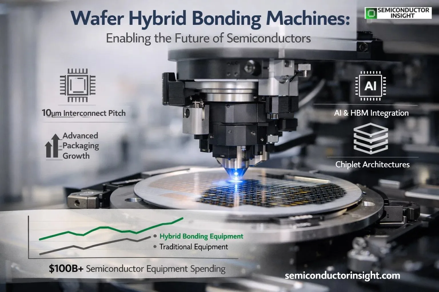
Wafer Hybrid Bonding Machine Market Unlocking High-Density 3D Integration in 2026
In the rapidly evolving semiconductor landscape, innovation is no longer confined to transistor scaling alone. The spotlight is steadily shifting toward advanced packaging technologies, where performance gains are achieved through smarter integration rather than just smaller nodes. At the centre of this transformation lies Wafer Hybrid Bonding Machine Market a niche yet powerful segment redefining how chips are assembled at the atomic level.
Hybrid bonding combines dielectric and metal bonding in a single process, enabling direct copper-to-copper interconnects without the need for traditional micro-bumps. This allows significantly higher interconnect density and lower resistance, making it a critical enabler for next-generation devices, particularly in AI, high-performance computing (HPC), and memory applications.
Precision Engineering Meets Moore’s Law Evolution
- As traditional scaling approaches the physical limits of Moore’s Law, hybrid bonding emerges as a complementary pathway.
- According to IEEE publications, hybrid bonding can achieve interconnect pitches below 10 microns far superior to conventional flip-chip bonding, which typically operates above 40 microns.
- This advancement is not just incremental it fundamentally changes chip architecture. Leading semiconductor manufacturers like TSMC have already integrated hybrid bonding into their 3D Fabric technology, enabling vertical stacking of logic and memory chips with unprecedented efficiency.
- Their annual reports highlight that advanced packaging now contributes a growing share of revenue, signalling a structural shift in semiconductor value chains.
Data-Backed Momentum across the Ecosystem
The demand for hybrid bonding machines is closely tied to the surge in advanced semiconductor applications. Data from SEMI indicates that global semiconductor equipment spending surpassed $100 billion in recent years, with advanced packaging equipment witnessing one of the fastest growth rates within the segment.
Additionally, insights from U.S. Department of Commerce emphasize that advanced packaging, including hybrid bonding, is becoming strategically critical for national semiconductor supply chains. Government-backed initiatives such as the CHIPS Act are allocating billions of dollars to strengthen domestic manufacturing capabilities, indirectly accelerating the adoption of cutting-edge bonding technologies.
The Rise of AI and High-Bandwidth Memory Integration
- The explosive growth of artificial intelligence is placing enormous pressure on chip performance and energy efficiency. Hybrid bonding plays a pivotal role in enabling High-Bandwidth Memory (HBM) integration, where memory stacks are directly bonded to logic chips for faster data transfer.
For instance, Intel Corporation has been actively advancing its Foveros Direct technology, which utilizes hybrid bonding to achieve fine-pitch interconnects. According to Intel’s technical disclosures, this approach reduces latency while improving power efficiency two critical parameters for AI workloads.
- Similarly, developments documented in Nature Electronics highlight that hybrid bonding can reduce interconnect energy consumption by up to 30% compared to traditional methods, making it highly relevant in sustainability-focused semiconductor design.
For additional report info, feel free to view our most recent edition: https://semiconductorinsight.com/report/wafer-hybrid-bonding-machine-market/
Manufacturing Complexity and Technological Sophistication
Despite its advantages, hybrid bonding is not a straightforward upgrade it demands extreme precision. The process requires atomically clean surfaces, sub-nanometer alignment accuracy, and defect-free wafer interfaces. Even minor contamination can lead to bonding failures, impacting yield.
This is where wafer hybrid bonding machines become indispensable. These systems integrate advanced alignment optics, plasma activation, and ultra-clean environments to ensure consistent bonding quality. Equipment manufacturers are investing heavily in automation and AI-driven inspection systems to meet these stringent requirements.
According to technical papers from MIT, maintaining surface roughness below 0.5 nanometers is crucial for successful hybrid bonding a benchmark that underscores the engineering sophistication involved.
A Shift toward Chiplet-Based Architectures
- Another defining trend shaping this market is the industry-wide move toward chiplet architectures. Instead of building a single monolithic chip, manufacturers are designing smaller functional units (chiplets) and integrating those using advanced bonding techniques.
- Hybrid bonding provides the interconnect density needed to make chiplets behave like a single unified system. This approach not only improves manufacturing yield but also enhances design flexibility, allowing companies to mix and match different process nodes within a single package.
- Organizations such as DARPA have been actively funding research programs focused on heterogeneous integration, further reinforcing the importance of hybrid bonding technologies in future semiconductor design.
Why This Market Matters More Than Ever
Wafer Hybrid Bonding Machine Market is more than simply another type of equipment; it is a key part of the next stage of semiconductor innovation. As companies need semiconductors that are faster, smaller, and use less energy, hybrid bonding becomes more and more important.
This technology is quietly changing the future of electronics by making AI accelerators possible, supporting new memory architectures, and driving chiplet ecosystems. What makes it so interesting is that it can close the gap between performance needs and physical limits, which has been a problem in the semiconductor industry for a long time.
In short, even though people may never see these devices, they will have an effect on every smart device, data center, and new technology that makes up the digital age.

Comments (0)