
Key Statistics
Key Takeaways
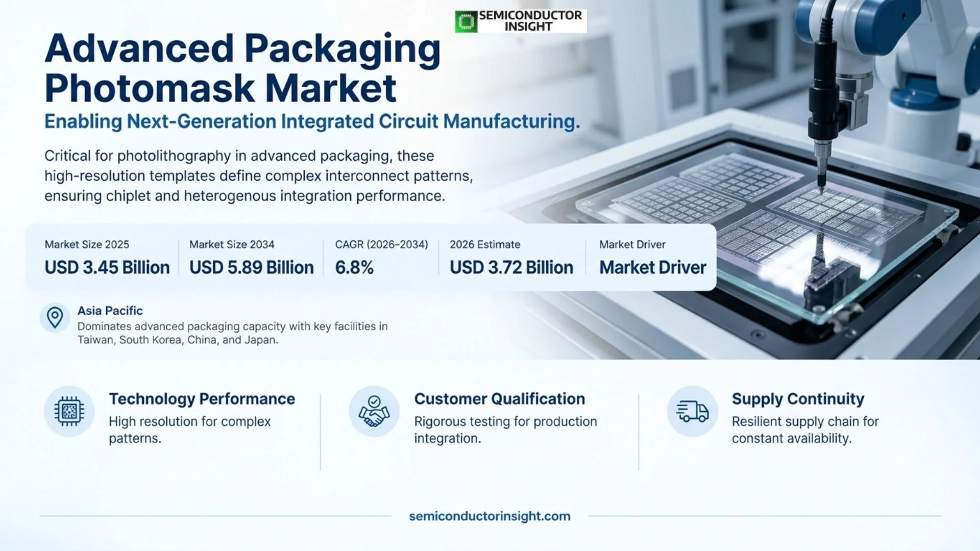
- Market size and growth: the market is valued at USD 3.72 billion in 2026 and is projected to reach USD 5.89 billion by 2034, representing a 6.8% CAGR during 2026–2034.
- Quartz masks dominate because advanced packaging requires high dimensional stability, durability and pattern fidelity across fine-pitch redistribution and interconnect layers.
- 3D IC, fan-out WLP and 2.5D packaging are the most important growth applications as AI accelerators and chiplets increase interconnect density and overlay requirements.
- Asia Pacific leads through Taiwan, South Korea, China and Japan, where foundries, OSATs and mask shops operate close to the largest advanced-packaging production clusters.
- AI-driven semiconductor investment is expanding the addressable base: SEMI projected global 300mm fab equipment spending of USD 133 billion in 2026 and USD 151 billion in 2027, supporting leading-edge logic and packaging ecosystems.
Advanced Packaging Photomask Market Overview
Advanced Packaging Photomask Market was valued at USD 3.45 billion in 2025 and is estimated at USD 3.72 billion in 2026. The market is projected to reach USD 5.89 billion by 2034, representing a CAGR of 6.8% during 2026–2034. Asia Pacific is the largest regional market because Taiwan, South Korea, China and Japan combine advanced packaging, foundry, OSAT and photomask manufacturing capacity.
Base year: 2025 · Estimated year: 2026 · Forecast period: 2026–2034 · Values in USD million unless otherwise stated
Advanced packaging photomasks are patterned quartz or soda-lime substrates used to transfer redistribution, bump, interposer and other package-level circuit patterns during lithography. Unlike front-end masks for transistor fabrication, these masks support wafer-level and panel-level packaging processes such as fan-out, 2.5D interposers, 3D IC integration and flip chip. As package feature sizes shrink and layer counts increase, mask dimensional stability, defect control and turnaround time become increasingly important to packaging yield.
The demand cycle is being accelerated by AI and heterogeneous integration. Large processors and HBM stacks increasingly rely on chiplets, high-density redistribution layers and advanced interposers because scaling a single monolithic die is costly and technically difficult. This creates more lithography steps inside packaging and raises mask complexity. Photomask suppliers that can provide fine critical dimensions, tight placement accuracy and rapid engineering turns are therefore gaining importance within the advanced-packaging ecosystem.
Asia Pacific dominates production because Taiwan, South Korea, China and Japan combine foundries, OSATs, packaging houses and photomask manufacturers. North America is expanding advanced-packaging investment for AI and semiconductor localization, while Europe focuses on automotive, power and high-reliability applications. The market remains technically concentrated because mask writers, inspection tools and process know-how create high barriers to entry, particularly for high-end quartz masks.
Segment Analysis: By Type
By type, the market is segmented into quartz masks and soda masks. Quartz masks lead because they provide stronger thermal stability, lower distortion and higher precision for fine packaging features. Soda-lime masks remain relevant where feature sizes and overlay requirements are less demanding and cost sensitivity is higher. As packaging moves toward denser redistribution, hybrid bonding and chiplet integration, a larger share of mask value shifts toward higher-specification quartz products.
| Type | Technical / commercial role | Market position |
|---|---|---|
| Quartz Mask | High dimensional stability and precision for fine-pitch advanced packaging. | Largest segment; strongest fit for high-end 2.5D, 3D and fan-out applications. |
| Soda Mask | Lower-cost substrate for less demanding lithography layers and mature packaging processes. | Cost-sensitive segment; retained where feature size and distortion tolerance allow. |
Segment Analysis: By Application
Applications include 3D IC, FO SiP, FO WLP, 3D WLP, WLCSP, 2.5D and flip chip. 3D IC and fan-out formats provide the strongest growth because AI, HPC and compact consumer devices require higher interconnect density. Flip chip remains a large installed base, while 2.5D interposers are critical for combining large accelerators with HBM. Each additional redistribution or bonding layer can require dedicated mask sets, increasing mask intensity per package.
| Application | Demand characteristics |
|---|---|
| 3D IC | Vertical die integration and hybrid bonding require tight overlay and fine patterns. |
| FO SiP | Fan-out system-in-package integrates multiple components with dense redistribution. |
| FO WLP | High-growth packaging for mobile, RF and compute devices requiring advanced RDL masks. |
| 3D WLP | Adds vertical connectivity and wafer-level stacking complexity. |
| WLCSP | High-volume compact packaging with established photolithography steps. |
| 2.5D | Interposers connect logic and HBM for AI/HPC, increasing mask complexity and value. |
| Flip Chip | Large installed packaging base supporting bump and redistribution patterning. |
Segment Analysis: By End User
End users include IDMs, foundries and OSATs. Foundries are increasingly important because leading companies have expanded from wafer fabrication into integrated advanced-packaging services, especially for AI accelerators and chiplets. OSATs remain major consumers across fan-out and system-in-package applications, while IDMs use advanced masks for captive packaging flows and specialized products. Purchasing decisions emphasize defect density, turnaround time, pattern placement and the mask supplier’s ability to support rapid design revisions.
| End User | Demand logic |
|---|---|
| IDMs | Captive packaging flows and specialized high-reliability devices. |
| Foundries | Rapidly growing integrated packaging services for AI, HPC and chiplets. |
| OSATs | High-volume outsourced assembly across fan-out, WLCSP, 2.5D and SiP. |
Segment Analysis: By Technology Node
Packaging photomask demand can also be segmented by the node of the underlying semiconductor and the feature density required in package interconnects. Products associated with sub-16nm logic and leading AI accelerators require the most advanced packaging because die sizes, I/O density and HBM interfaces are highest. Mature-node devices continue to use conventional masks and lower-cost package structures, but the value per mask rises materially as interconnect pitch and overlay tolerances tighten.
| Technology Node | Market significance |
|---|---|
| >28nm | Mature-node and cost-sensitive packaging with established mask specifications. |
| 16–28nm | Intermediate complexity across communications, automotive and mixed-signal devices. |
| <16nm | Highest mask complexity; strong link to advanced logic, AI and heterogeneous integration. |
Regional Analysis
Asia Pacific dominates the advanced packaging photomask market because the region contains the majority of advanced packaging capacity and a dense photomask supply chain. Taiwan leads in foundry and high-end packaging, South Korea combines memory and advanced integration, China is expanding domestic mask capacity, and Japan remains strong in materials and photomask technology. North America is growing through AI packaging investment and semiconductor localization.
Advanced packaging photomasks have strong geographic clustering because mask turnaround time matters during process development and high-volume production. Fabs and OSATs benefit from nearby mask shops that can respond quickly to design changes and defects. Asia Pacific therefore has a structural advantage from proximity between customers, writers, inspection tools and material suppliers. Regional diversification is increasing, but replicating this ecosystem requires specialized capital equipment and experienced process engineering.
| Region | Position | Growth outlook | Demand profile | Supplier-selection factor |
|---|---|---|---|---|
| Asia Pacific | Largest | High | Foundry, OSAT and mask clusters | Precision, turnaround and capacity |
| North America | High-value growth | High | AI/HPC packaging and localization | Technology and domestic support |
| Europe | Established niche | Moderate | Automotive, industrial and power | Reliability and specialty masks |
| South America | Nascent | Low-Moderate | Assembly and research | Cost and imported supply |
| Middle East & Africa | Emerging | Low-Moderate | Semiconductor infrastructure projects | Technology transfer and support |
Competitive Landscape
Competition in the Advanced Packaging Photomask market is shaped by technology performance, customer qualification, application engineering and continuity of supply. Leading companies use product breadth and global support to win large programs, while specialist suppliers can defend attractive niches through deeper technical performance in specific applications. As the market expands, customers increasingly evaluate total system value and lifecycle support rather than relying only on initial component price.
The leading suppliers compete through a combination of proprietary technology, manufacturing scale and customer relationships. In the Advanced Packaging Photomask market, design wins can remain in place for several product generations because switching suppliers often requires requalification, software changes or manufacturing adjustments. This creates durable revenue positions for vendors that deliver reliable performance and responsive technical support.
Regional suppliers can still gain share where local availability, cost and fast engineering response matter. Their strongest opportunities are generally in standardized or mature applications, while the highest-performance segments remain concentrated among companies with deeper intellectual property, process control and qualification histories. This creates a market structure with both global platform leaders and specialized regional competitors.
Competitive strategy is increasingly moving toward integrated solutions. Customers prefer suppliers that can combine the core product with software, interface components, testing, support or adjacent technologies because integration reduces project risk and development time. Companies able to solve a broader customer problem therefore have more pricing power than vendors competing only on a single specification.
| Competitive tier | Representative companies | Competitive basis |
|---|---|---|
| Global technology leaders | Photronics, Toppan, DNP, ShenZheng QingVi | Scale, broad product portfolios, strong R&D and global customer support. |
| Established specialists | Taiwan Mask, Nippon Filcon, Compugraphics, Newway Photomask | Application-specific engineering and strong qualification in selected segments. |
| Regional / emerging suppliers | Shenzhen Longtu Photomask, Wuxi Zhongwei Mask Electronics, CR Micro, SMIC-Mask Service | Local service, competitive pricing and focused customer relationships. |
Key Participants
The profiled competitive set includes Photronics, Toppan, DNP, ShenZheng QingVi, Taiwan Mask, Nippon Filcon, Compugraphics, Newway Photomask, Shenzhen Longtu Photomask, Wuxi Zhongwei Mask Electronics, CR Micro, SMIC-Mask Service. Supplier position depends on engineering performance, customer qualification, manufacturing continuity and the ability to support design changes over long product cycles. Larger vendors benefit from broad portfolios and application teams, while specialists can retain strong positions in narrow, technically demanding subsegments where historical qualification and process know-how create meaningful switching costs.
Production Capacity Analysis
Production capacity for Advanced Packaging Photomask is constrained by the combination of specialized equipment, qualified materials, process know-how and customer-specific validation. Nominal factory output can overstate commercial supply because a new line or material source must often demonstrate consistent performance before it can serve high-value customers. This makes qualified capacity more important than raw nameplate capacity.
Regional manufacturing and service capacity influence lead time and resilience. Customers increasingly prefer suppliers that can support major production clusters from more than one site, reducing exposure to logistics disruption and single-factory events. At the same time, duplicating specialized processes can be difficult because equipment recipes, trained engineers and quality systems must be transferred without changing product performance.
The strongest capacity investments are aligned with structural demand drivers rather than short-term cycles. Suppliers expanding around AI, advanced semiconductor manufacturing, automotive electronics or industrial automation seek to secure positions before customer volumes scale. Effective capacity therefore includes engineering resources, test capability and local technical support in addition to physical manufacturing equipment.
| Capacity factor | Market implication |
|---|---|
| Specialized manufacturing | Determines qualified output and technical performance. |
| Critical materials / components | Can constrain supply despite available factory floor space. |
| Qualification and test | Controls how quickly new capacity becomes usable by customers. |
| Regional support | Improves lead time, resilience and customer retention. |
Market Dynamics
The Advanced Packaging Photomask market is driven by higher system performance, automation, digitalization and expanding use in high-value applications. Growth is moderated by development cost, qualification requirements and supply-chain concentration. The strongest opportunities occur where new architectures or applications create a clear performance advantage and where suppliers can reduce integration complexity for customers.
MARKET DRIVERS
| Driver | Relative impact | Commercial mechanism |
|---|---|---|
| Structural end-market growth | High | Expanding deployments increase unit demand and installed-base requirements. |
| Technology upgrade cycle | High | Higher performance raises value per product and accelerates replacement. |
| Customer integration needs | Medium-High | Validated solutions reduce engineering time and project risk. |
| Regional capacity expansion | Medium | New manufacturing clusters create local supplier demand. |
Structural end-market expansion
Growth in the Advanced Packaging Photomask market is supported by rising deployment across its principal applications. Customers are investing because the technology improves performance, efficiency, automation or product capability in ways that are difficult to replicate with older approaches. This expands both new-system demand and the installed base that later requires replacement, upgrades or related services.
Higher technical requirements increase value per system
New product generations demand tighter performance, greater integration and better reliability. These requirements can increase selling prices even when unit volumes grow more slowly, because customers are willing to pay for solutions that protect yield, uptime or user experience. Suppliers with stronger engineering capability therefore benefit disproportionately from technology transitions.
Regional investment broadens customer access
Manufacturing and infrastructure investment in North America, Europe and Asia is creating additional customer clusters outside traditional centers. Local engineering support and shorter supply chains help suppliers qualify products earlier in new projects, creating an opportunity to win design positions before production reaches full scale.
MARKET RESTRAINTS
| Restraint | Relative impact | Commercial mechanism |
|---|---|---|
| Development and qualification cost | High | Raises barriers to entry and lengthens customer adoption. |
| Supply-chain concentration | Medium-High | Critical components or materials can limit output. |
| Price pressure | Medium | Customers seek lower total system cost as volumes increase. |
| Technology substitution | Medium | Alternative architectures can replace incumbent solutions in selected uses. |
Qualification slows supplier switching
Customers in technical markets cannot change suppliers based only on purchase price. New products must demonstrate performance, reliability and compatibility in the actual application, which can require months of engineering work. This limits the pace at which new entrants gain share and can delay commercialization of technically promising products.
Specialized inputs can constrain supply
Advanced products depend on a limited number of qualified materials, components or manufacturing tools. Shortages or long lead times at one upstream stage can restrict finished-product output even when downstream assembly capacity is available. Suppliers therefore carry strategic inventory or qualify alternate sources, but those actions increase cost.
Customer cost pressure remains persistent
As a technology becomes more widely adopted, customers expect lower unit costs and may redesign systems to use standardized components. Suppliers must offset this pressure through better performance, lower manufacturing cost and additional software or service value. Vendors that cannot maintain differentiation can face margin erosion even in a growing market.
MARKET OPPORTUNITIES
High-performance product generations
New architectures create opportunities for premium products that solve tighter performance, efficiency or integration requirements.
Localized supply and technical support
Customers increasingly value shorter lead times and regional engineering, especially for production-critical components.
Software and data-enabled services
Monitoring, analytics and updateable software can create recurring value beyond the initial hardware sale.
Emerging end-use applications
New industries and use cases can broaden the addressable market beyond the traditional customer base.
Supply Chain Analysis
Specialized materials and components
Core product manufacturing
Qualification and system integration
End-user deployment, service and replacement
The upstream supply chain provides the specialized materials, semiconductor devices, mechanical components or substrates that determine baseline product performance. Qualified inputs are important because changes in composition or manufacturing source can alter reliability, electrical behavior or process compatibility. Suppliers therefore maintain close technical relationships with upstream partners and often approve alternate sources before a disruption occurs.
Manufacturing converts these inputs into finished products using process-specific equipment, inspection and test. Quality systems are central because customers expect lot-to-lot consistency and traceability, particularly in semiconductor, automotive and industrial applications. High-value suppliers differentiate through process control rather than simple assembly scale, and they invest heavily in metrology or validation to protect yield.
Downstream value is created when the product is integrated into the customer system and validated under real operating conditions. Application engineers support installation, software, calibration or process optimization, while service teams maintain the installed base. This lifecycle relationship creates recurring revenue through replacement, updates, refurbishment or expansion and makes customer support an important part of the market structure.
Recent Developments
1 Apr 2026 – SEMI projects double-digit growth in 300mm fab equipment spending
SEMI forecast global 300mm fab equipment spending of USD 133 billion in 2026 and USD 151 billion in 2027, citing AI and advanced-node demand. The investment cycle supports the logic and memory devices that increasingly require advanced packaging and high-precision package lithography. Source
2026 – Photronics continues global advanced photomask support
Photronics markets leading-edge advanced photomasks across multiple mask formats and lithography applications, reflecting ongoing investment in global mask capability and rapid-turn solutions for semiconductor customers. Source
REPORT SCOPE & SEGMENTATION
| Base Year | 2025 |
| Estimated Year | 2026 |
| Forecast Year | 2034 |
| 2025 Market Size | USD 3.45 billion |
| 2026 Market Size | USD 3.72 billion |
| 2034 Market Size | USD 5.89 billion |
| CAGR | 6.8% during 2026–2034 |
| Largest Market / Leading Geography | Asia Pacific |
| By Type | Quartz Mask; Soda Mask |
| By Application | 3D IC; FO SiP; FO WLP; 3D WLP; WLCSP; 2.5D; Flip Chip |
| By End User | IDMs; Foundries; OSATs |
| By Technology Node | >28nm; 16–28nm; <16nm |
| Key Companies | Photronics; Toppan; DNP; ShenZheng QingVi; Taiwan Mask; Nippon Filcon; Compugraphics; Newway; Shenzhen Longtu; Wuxi Zhongwei; CR Micro; SMIC-Mask Service |
Frequently Asked Questions
What is the size of the advanced packaging photomask market?
The market is valued at USD 3.72 billion in 2026 and is projected to reach USD 5.89 billion by 2034, representing a 6.8% CAGR during 2026–2034. The 2025 market size is USD 3.45 billion.
Which photomask type leads the market?
Quartz masks lead because advanced packaging requires high dimensional stability, pattern accuracy and durability across fine-pitch redistribution and interconnect layers.
Which applications drive growth?
3D IC, 2.5D interposers, fan-out wafer-level packaging and chiplet integration are the main growth drivers because AI and HPC devices require dense interconnects and HBM integration.
Which region leads the market?
Asia Pacific leads because Taiwan, South Korea, China and Japan contain the strongest concentration of foundries, OSATs, advanced packaging lines and photomask suppliers.
Why does advanced packaging require specialized masks?
Fine redistribution lines, multiple package layers and tight overlay tolerances require better pattern placement, defect control and dimensional stability than many conventional packaging processes.
What are the main constraints?
Mask-writer capital intensity, high-end inspection requirements, customer concentration and the regional concentration of advanced packaging capacity are the main constraints.
Research Sources & Evidence Base
Get Sample Report PDF for Exclusive Insights
Report Sample Includes
- Table of Contents
- List of Tables & Figures
- Charts, Research Methodology, and more...
 Download Sample Report PDF