MARKET INSIGHTS
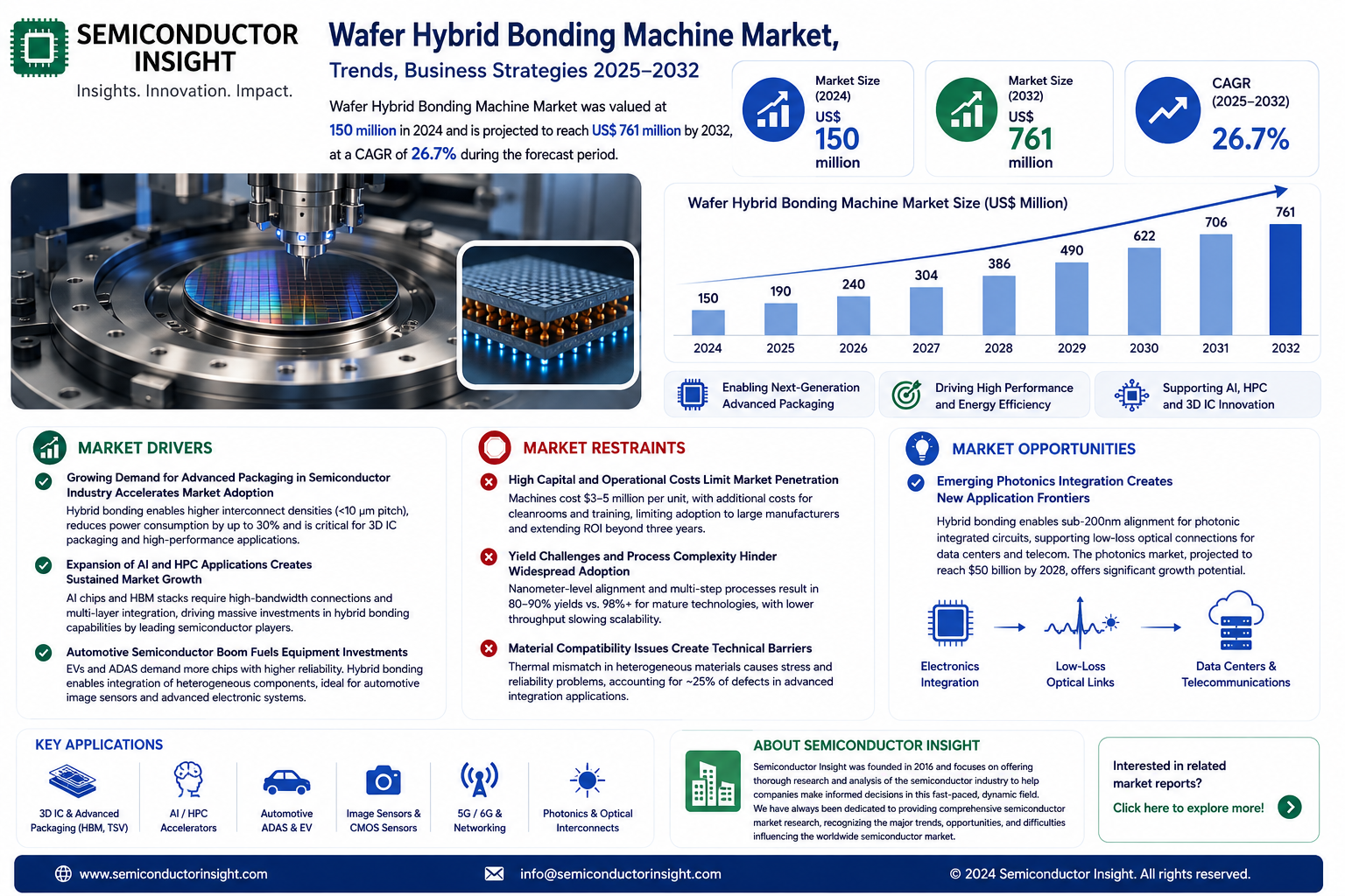
The global Wafer Hybrid Bonding Machine Market was valued at 150 million in 2024 and is projected to reach US$ 761 million by 2032, at a CAGR of 26.7% during the forecast period.
Wafer hybrid bonding machines are advanced semiconductor manufacturing equipment designed to facilitate hybrid bonding—a process combining dielectric bonding (SiOx) with embedded metal (Cu) interconnections. This technology enables higher I/O density, improved electrical performance, and reduced power consumption compared to traditional through-silicon vias (TSVs). These machines are critical for producing high-performance 3D ICs, CMOS image sensors, memory devices, and other semiconductor components requiring ultra-fine pitch bonding.
The market is expanding rapidly due to rising demand for miniaturized and high-performance semiconductors in applications like artificial intelligence, 5G, and automotive electronics. Key players such as EV Group (EVG), SUSS MicroTec, and ASMPT are investing in advanced bonding technologies to address the growing need for heterogeneous integration. For instance, in 2023, EVG launched its latest hybrid bonding platform, enhancing throughput and alignment precision for next-generation logic and memory devices.
MARKET DYNAMICS
MARKET DRIVERS
Growing Demand for Advanced Packaging in Semiconductor Industry Accelerates Market Adoption
The semiconductor industry’s shift towards advanced packaging technologies is driving significant demand for wafer hybrid bonding machines. With the global semiconductor packaging market projected to surpass $50 billion by 2025, hybrid bonding has emerged as a critical solution for achieving higher interconnect densities and improved performance. Major semiconductor foundries are increasingly adopting hybrid bonding for 3D IC packaging, as it enables stacking of chips with interconnect pitches below 10 microns – a capability that traditional bonding methods cannot match. This technology’s ability to reduce power consumption by up to 30% while increasing bandwidth makes it particularly valuable for high-performance computing applications.
Expansion of AI and HPC Applications Creates Sustained Market Growth
Artificial intelligence and high-performance computing applications are creating unprecedented demand for wafer hybrid bonding solutions. The AI chip market, expected to grow at over 35% CAGR through 2030, requires advanced packaging techniques to meet the performance demands of neural networks and machine learning processors. Hybrid bonding enables the creation of high-bandwidth memory (HBM) stacks that are essential for AI accelerators, with current HBM3 implementations requiring up to 16 layers of stacked memory dies. Leading semiconductor manufacturers are investing heavily in hybrid bonding capabilities to support these applications, with several major players announcing billion-dollar fab expansions specifically targeting advanced packaging capabilities.
Automotive Semiconductor Boom Fuels Equipment Investments
The automotive semiconductor market, projected to reach $80 billion by 2028, is creating new opportunities for wafer hybrid bonding technology. Modern vehicles incorporate hundreds of semiconductors for ADAS, infotainment, and powertrain control, with electric vehicles requiring nearly twice as many chips as conventional vehicles. Hybrid bonding is particularly valuable for automotive applications because of its reliability under extreme conditions and ability to integrate heterogeneous components. The technology’s adoption in automotive image sensors has grown rapidly, with CMOS image sensors for autonomous vehicles requiring pixel sizes below 2 microns – a specification that hybrid bonding is uniquely positioned to support.
MARKET RESTRAINTS
High Capital and Operational Costs Limit Market Penetration
Wafer hybrid bonding machines represent a significant capital investment, with prices ranging from $3-5 million per unit depending on configuration and capabilities. The total cost of ownership is further increased by the need for cleanroom facilities and specialized operator training. These high barriers to entry effectively limit adoption to large semiconductor manufacturers and foundries, leaving smaller players unable to justify the investment. Even among leading manufacturers, the return on investment period for hybrid bonding equipment typically exceeds three years, making it challenging to scale production capacity rapidly.
Yield Challenges and Process Complexity Hinder Widespread Adoption
Despite technological advancements, hybrid bonding still faces yield challenges that impact production economics. The multi-step bonding process requires nanometer-level alignment accuracy, with even minor variations in temperature or pressure potentially causing defects. Current production yields for advanced hybrid bonding processes typically range between 80-90%, compared to 98%+ yields for mature packaging technologies. The complexity of the bonding process also creates challenges in scaling production volumes, with throughput rates for hybrid bonding machines significantly lower than conventional packaging equipment.
Material Compatibility Issues Create Technical Barriers
The expansion of hybrid bonding to new applications is constrained by material compatibility challenges. Different wafer materials exhibit varying coefficients of thermal expansion, which can lead to stress and reliability issues in the bonded structure. This is particularly problematic for emerging applications in photonics and MEMS, where dissimilar materials must be integrated. Recent research indicates that thermal mismatch problems account for nearly 25% of hybrid bonding defects in heterogeneous integration applications, highlighting the need for continued process development.
MARKET OPPORTUNITIES
Emerging Photonics Integration Creates New Application Frontiers
The growing photonics market, expected to reach $50 billion by 2028, presents significant opportunities for hybrid bonding adoption. Photonic integrated circuits require precise alignment of optical components that hybrid bonding can provide, enabling the integration of lasers, modulators, and detectors on a single chip. Recent breakthroughs have demonstrated hybrid bonding of silicon photonics chips with sub-200nm alignment accuracy, a critical requirement for optical interconnects in data centers and telecommunications. The technology’s ability to create low-loss optical connections between chips is driving interest from major cloud service providers and network equipment manufacturers.
Chiplet Adoption Revolution Creates Demand for Advanced Bonding Solutions
The semiconductor industry’s shift toward chiplet-based designs is creating new opportunities for hybrid bonding technology. Chiplet architectures, which combine multiple specialized dies in a single package, require high-density interconnects that hybrid bonding can provide. Industry consortia have established standards for chiplet interfaces that assume hybrid bonding capabilities, with interconnect pitches expected to shrink below 2 microns in next-generation designs. Leading CPU and GPU manufacturers have already announced products utilizing hybrid bonding for chiplet integration, signaling strong future demand for bonding equipment.
Advanced Memory Architectures Drive Technology Innovation
The evolution of memory technologies is creating new applications for hybrid bonding in advanced memory stacks. Emerging memory architectures such as Compute Express Link (CXL) and high-bandwidth memory (HBM) increasingly rely on hybrid bonding to achieve the required interconnect densities. Memory manufacturers are developing new processes specifically for hybrid-bonded stacks, with some latest-generation HBM designs requiring over 100,000 interconnects per square millimeter. This trend is expected to accelerate as AI workloads push memory bandwidth requirements beyond current capabilities, creating sustained demand for advanced bonding solutions.
WAFER HYBRID BONDING MACHINE MARKET TRENDS
Advancements in Semiconductor Packaging to Drive Demand for Hybrid Bonding Machines
The wafer hybrid bonding machine market is gaining significant traction due to the rising adoption of advanced packaging technologies such as 3D ICs, chiplet integration, and heterogeneous integration. With semiconductor manufacturers striving to achieve higher performance while reducing power consumption, hybrid bonding has emerged as a critical enabler. The technology facilitates direct copper-to-copper interconnects, which offer lower resistance and higher I/O density compared to traditional through-silicon vias (TSVs). As a result, leading foundries and memory manufacturers are increasingly incorporating hybrid bonding techniques to enhance device performance in applications like high-bandwidth memory (HBM) and CMOS image sensors.
Other Trends
Expansion of 5G and AI Infrastructure
The ongoing rollout of 5G networks and the proliferation of artificial intelligence (AI) applications are generating substantial demand for wafer hybrid bonding machines. Increased data processing requirements necessitate high-performance semiconductor packages with superior interconnect density. Hybrid bonding enables tighter integration between logic and memory chips, which is essential for AI accelerators and networking equipment. Additionally, applications in edge computing and autonomous systems further reinforce the need for compact, high-performance chips produced using hybrid bonding.
Growth in Automotive and IoT Applications
The automotive sector is witnessing a surge in demand for hybrid-bonded semiconductor devices due to the increasing integration of advanced driver-assistance systems (ADAS) and electric vehicle (EV) powertrains. These applications require highly reliable and miniaturized electronic components, making hybrid bonding an attractive solution. Similarly, the expansion of the Internet of Things (IoT) ecosystem has led to heightened demand for low-power, compact chips that can be efficiently manufactured using hybrid bonding techniques. This trend is particularly prominent in smart sensors and wearable devices, where performance and energy efficiency are paramount.
COMPETITIVE LANDSCAPE
Key Industry Players
Semiconductor Equipment Leaders Drive Innovation in Hybrid Bonding Technology
The wafer hybrid bonding machine market features a moderately consolidated competitive environment with established semiconductor equipment manufacturers dominating the landscape. EV Group (EVG) has emerged as the technology leader, capturing an estimated 32% market share in 2024 through its advanced GEMINI® hybrid bonding systems that enable sub-micron alignment accuracy critical for 3D IC applications.
European firms SUSS MicroTec and ASMPT represent significant competitors, collectively accounting for nearly 28% of global revenues. Their strong position stems from patented bonding technologies that address critical challenges in wafer-level packaging for memory and logic devices.
Asia-based manufacturers are rapidly gaining traction, with Beijing U-Precision Tech and Piotech expanding their footprint. These companies benefit from localized semiconductor supply chains and government incentives supporting equipment manufacturing. Their competitive pricing strategies and responsive technical support have enabled successful penetration in emerging markets.
The market has seen notable technological convergence as players integrate artificial intelligence for process optimization and predictive maintenance in newer equipment models. Wisdom Semiconductor Technology recently introduced machine learning algorithms that reduce bonding defects by analyzing process parameters in real-time – a development expected to set new industry benchmarks.
List of Key Wafer Hybrid Bonding Machine Manufacturers
- EV Group (EVG) (Austria)
- SUSS MicroTec (Germany)
- Genesem (South Korea)
- ASMPT (Singapore)
- C SUN (Taiwan)
- Piotech (China)
- Beijing U-Precision Tech (China)
- Wisdom Semiconductor Technology (China)
Wafer Hybrid Bonding Machine Market Segment Analysis
By Type
Wafer-to-Wafer Hybrid Bonding Dominates Due to High-Density Integration in Semiconductor Manufacturing
The market is segmented based on type into:
- Wafer-to-Wafer Hybrid Bonding
- Die-to-Wafer Hybrid Bonding
By Application
CMOS Image Sensors Lead the Market Owing to Increased Demand in Smartphones and Automotive Cameras
The market is segmented based on application into:
- CMOS Image Sensor (CIS)
- NAND Flash Memory
- DRAM
- High Bandwidth Memory (HBM)
- Others
By End-Use Industry
Consumer Electronics Accounts for Largest Share Due to Proliferation of 5G Devices and Wearables
The market is segmented based on end-use industry into:
- Consumer Electronics
- Automotive
- Healthcare
- Industrial
- Aerospace & Defense
By Bonding Technology
Copper Hybrid Bonding Gains Traction for High-Performance Computing Applications
The market is segmented based on bonding technology into:
- Oxide Hybrid Bonding
- Copper Hybrid Bonding
- Hybrid Cu/Oxide Bonding
Regional Analysis: Wafer Hybrid Bonding Machine Market
Asia-Pacific
The Asia-Pacific region, led by China, Japan, and South Korea, dominates the global wafer hybrid bonding machine market due to its robust semiconductor manufacturing ecosystem. China’s aggressive investments in domestic chip production, including its $150 billion push to achieve semiconductor self-sufficiency, are fueling demand for advanced wafer bonding technologies. With over 60% of global semiconductor production occurring in the region, hybrid bonding adoption is accelerating for applications like 3D NAND and high-bandwidth memory (HBM) production. While cost sensitivity remains a concern, government initiatives and local manufacturers like Piotech and Beijing U-Precision Tech are driving accessibility. The region’s growing consumer electronics, automotive semiconductor, and 5G infrastructure sectors further stimulate market expansion.
North America
North America’s wafer hybrid bonding machine market is propelled by cutting-edge R&D in high-performance computing (HPC), AI chips, and quantum computing. The U.S. holds over 40% of the regional market share, with major semiconductor firms investing heavily in advanced packaging to maintain technological leadership. The CHIPS and Science Act has allocated $52 billion to bolster domestic semiconductor manufacturing, indirectly supporting hybrid bonding adoption. While the high cost of equipment limits uptake among smaller players, companies like Intel and Micron are driving demand for wafer-to-wafer bonding solutions in next-generation memory and logic devices. Collaborations between equipment suppliers and research institutions further accelerate technical advancements.
Europe
Europe’s market is characterized by specialized applications in automotive, industrial IoT, and MEMS sensors, with Germany and the Netherlands as key contributors. The region’s strength in photonics and automotive SiPs (System-in-Package) is driving selective adoption of hybrid bonding, particularly for CMOS image sensors in advanced driver-assistance systems (ADAS). EU-funded initiatives like the Chips Joint Undertaking are fostering innovation, though market growth is constrained by fragmented semiconductor manufacturing capacity. Local players like EV Group (EVG) and SUSS MicroTec hold technological expertise but face competition from Asian and American suppliers in scaling production.
Middle East & Africa
This emerging market shows nascent potential through strategic partnerships with global semiconductor firms establishing regional R&D hubs in countries like Israel and the UAE. While lacking significant local manufacturing, demand stems from defense electronics and telecommunications infrastructure projects. Hybrid bonding adoption remains limited by high equipment costs and the absence of a local supply chain, though government initiatives to develop tech ecosystems may gradually improve accessibility. The market is expected to grow in alignment with broader semiconductor industry investments in the region.
South America
South America’s wafer hybrid bonding machine market is in early development stages, with Brazil and Mexico showing limited uptake primarily in academic research and specialized industrial applications. Economic volatility and reliance on imported semiconductor components hinder widespread adoption. However, growing automotive electronics manufacturing and increasing foreign investments in electronics assembly present long-term opportunities. Market expansion will likely follow broader regional semiconductor industry maturation.
Report Scope
This market research report provides a comprehensive analysis of the Global Wafer Hybrid Bonding Machine market, covering the forecast period 2025–2032. It offers detailed insights into market dynamics, technological advancements, competitive landscape, and key trends shaping the semiconductor equipment industry.
Key focus areas of the report include:
- Market Size & Forecast: Historical data and future projections for revenue, unit shipments, and market value across major regions and segments. The market was valued at USD 150 million in 2024 and is projected to reach USD 761 million by 2032, growing at a CAGR of 26.7%.
- Segmentation Analysis: Detailed breakdown by product type (wafer-to-wafer and die-to-wafer hybrid bonding), application (CMOS Image Sensors, NAND, DRAM, HBM), and end-user industries (consumer electronics, automotive, healthcare).
- Regional Outlook: Insights into market performance across North America, Europe, Asia-Pacific, Latin America, and Middle East & Africa, with Asia-Pacific dominating due to semiconductor manufacturing hubs in China, Japan, and South Korea.
- Competitive Landscape: Profiles of leading market participants including EV Group (EVG), SUSS MicroTec, ASMPT, and Piotech, covering their product portfolios, manufacturing capacities, and strategic initiatives.
- Technology Trends & Innovation: Assessment of hybrid bonding advancements in 3D IC packaging, MEMS integration, and emerging applications in quantum computing and 5G technologies.
- Market Drivers & Restraints: Evaluation of factors including demand for advanced semiconductor packaging, miniaturization trends, and challenges like high capital investment and process complexity.
- Stakeholder Analysis: Strategic insights for semiconductor equipment manufacturers, foundries, IDMs, and investors regarding growth opportunities and market entry strategies.
The research methodology combines primary interviews with industry experts and analysis of verified market data from semiconductor equipment manufacturers, ensuring accuracy and reliability of market insights.
FREQUENTLY ASKED QUESTIONS:
What is the current market size of Global Wafer Hybrid Bonding Machine Market?
-> Wafer Hybrid Bonding Machine Market was valued at 150 million in 2024 and is projected to reach US$ 761 million by 2032, at a CAGR of 26.7% during the forecast period.
Which key companies operate in Global Wafer Hybrid Bonding Machine Market?
-> Key players include EV Group (EVG), SUSS MicroTec, ASMPT, Piotech, Beijing U-Precision Tech, and Wisdom Semiconductor Technology.
What are the key growth drivers?
-> Primary growth drivers include rising demand for 3D ICs, advanced packaging technologies, miniaturization of semiconductor devices, and growth in automotive electronics and MEMS applications.
Which region dominates the market?
-> Asia-Pacific leads the market due to strong semiconductor manufacturing presence, with China, Japan, and South Korea accounting for over 60% of global demand.
What are the emerging trends?
-> Emerging trends include adoption in quantum computing chips, integration with 5G and IoT devices, and development of hybrid bonding solutions for advanced memory applications like HBM.

Get Sample Report PDF for Exclusive Insights
Report Sample Includes
- Table of Contents
- List of Tables & Figures
- Charts, Research Methodology, and more...