
US CHIPS Act 2026 Progress: Fuelling Domestic Hardware Development Infrastructure
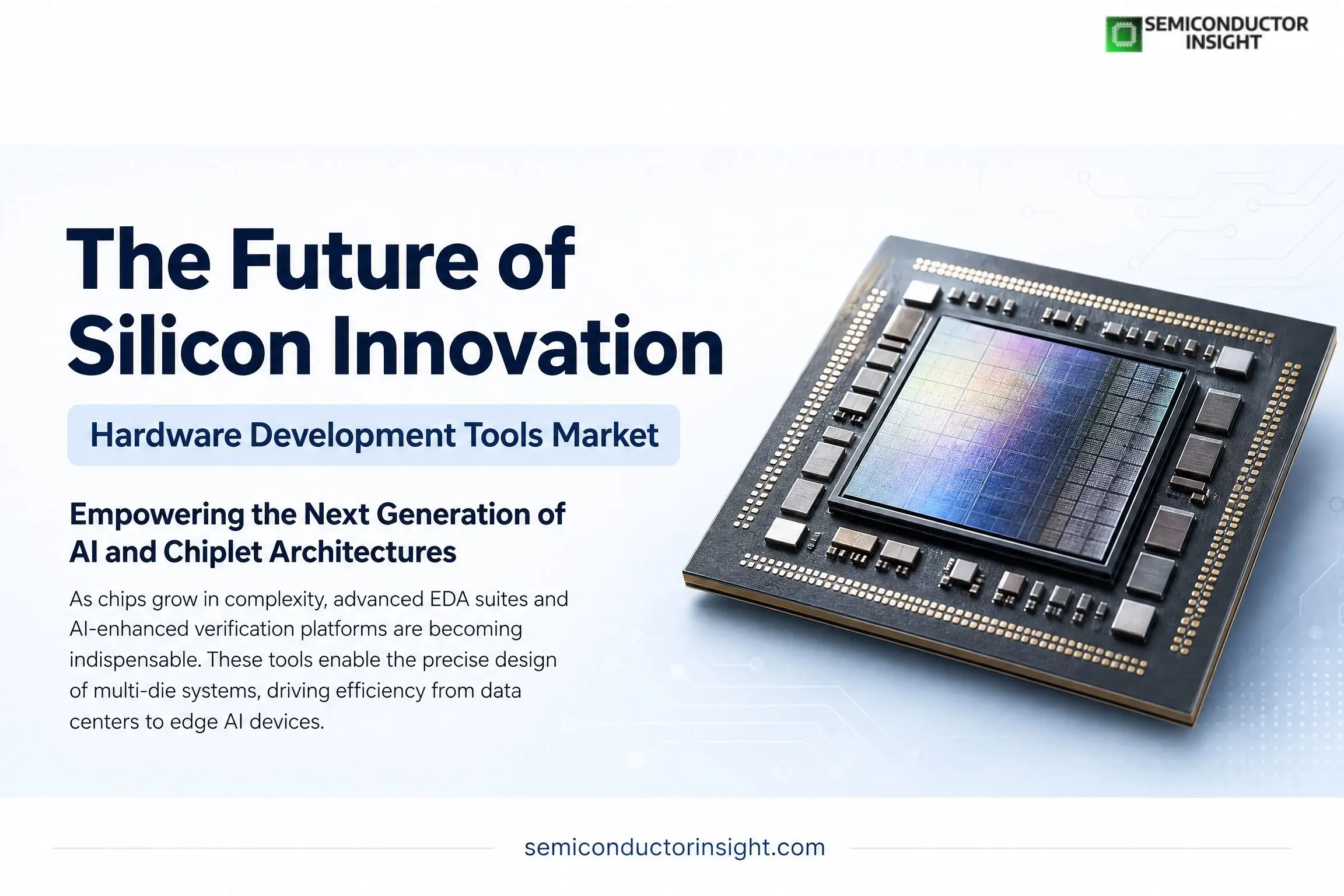
Hardware development tools in the semiconductor space encompass the sophisticated software suites, simulation environments, verification platforms, and specialized equipment that engineers rely on to create, test, and optimize integrated circuits before they ever reach a fabrication facility. These tools have become indispensable as chips grow more complex, with billions of transistors packed into designs for everything from data center processors to edge AI devices.
- The evolution traces back decades. In the early 1980s, companies spun out specialized EDA capabilities from larger electronics firms, marking the commercial birth of tools that could handle the exploding intricacy of modern semiconductors.
- Today, dominant players like Synopsys, Cadence, and Siemens EDA provide comprehensive flows covering everything from high-level synthesis to physical layout and sign-off. These platforms integrate hardware description languages such as Verilog and VHDL, enabling teams to simulate, verify, and iterate designs with precision that manual methods could never achieve.
- One standout area gaining momentum involves tools tailored for advanced process nodes and heterogeneous integration. As feature sizes shrink toward 3nm and below, design teams turn to AI-enhanced placement and routing solutions that optimize power, performance, and area metrics across massive multi-die systems. Cloud-based deployments have lowered barriers for smaller innovators, allowing scalable compute resources without massive upfront hardware investments.
- Government initiatives further amplify this shift. The CHIPS and Science Act has directed substantial resources toward bolstering U.S. research and design capabilities, including support for the National Semiconductor Technology Center.
- This public-private effort aims to accelerate innovation in areas like digital twins for chip simulation and advanced packaging metrology, helping reduce reliance on overseas supply chains while strengthening domestic expertise.
Exploring the Rise of Chiplet Architectures and Multi-Die Design Platforms
Chiplet-based designs represent a fundamental change in how hardware development tools are applied. Instead of monolithic dies, engineers now assemble smaller, specialized chiplets into a single package using high-bandwidth interconnects. Tools supporting 2.5D and 3D integration, including those handling through-silicon vias and hybrid bonding, have seen heightened adoption. These platforms allow for mixing different process technologiespairing a high-performance logic die with advanced memory, for instancewhile managing thermal and signal integrity challenges that come with denser packing.
Real-world examples abound in high-performance computing. Major GPU developers leverage sophisticated co-design environments to integrate high-bandwidth memory stacks directly with processing units, delivering the massive data throughput demanded by training large AI models. Automotive applications similarly benefit, where tools verify safety-critical systems across mixed analog-digital architectures. Case studies from industry collaborations highlight how early architectural exploration software helps evaluate trade-offs in power consumption and latency before committing to physical prototypes, shaving months off development cycles.
Power Semiconductor Tools: Enabling Efficiency in EVs and Renewables
- Beyond traditional logic design, hardware development extends into power electronics with specialized tools for wide-bandgap materials like silicon carbide (SiC) and gallium nitride (GaN).
- These semiconductors operate at higher voltages and temperatures with lower losses, making them ideal for electric vehicle inverters, fast chargers, and solar inverters. Design kits and simulation environments tailored for SiC MOSFETs and GaN HEMTs help engineers model switching behavior, thermal performance, and reliability under real-world stresses.
- In practice, automotive suppliers have deployed these tools to qualify devices for 800V architectures, improving vehicle range and charging speeds. One notable deployment involved power module development for next-generation EVs, where comprehensive multi-physics simulation caught potential failure modes early, and accelerating qualification for high-volume production.
- Renewable energy projects similarly utilize these platforms to optimize inverters that convert variable solar or wind input into stable grid power, contributing to broader energy transition goals.
The Open-Source Momentum and Collaborative Ecosystems
Parallel to commercial suites, open-source initiatives are carving out space in hardware development. Projects backed by organizations like DARPA and tech giants have produced full-stack toolchains, from synthesis to layout, lowering entry costs for academic researchers and startups. These efforts foster community-driven improvements in areas like routing algorithms and verification, complementing proprietary solutions rather than replacing them.
Universities and smaller fabs have adopted such stacks to prototype novel architectures, speeding experimentation in fields like quantum-adjacent computing or specialized sensors. This democratization encourages broader participation in semiconductor innovation, particularly as global demand for custom chips rises in everything from medical devices to aerospace systems.
Take a Quick Glance at Our In-Depth Analysis Report: https://semiconductorinsight.com/report/hardware-development-tools-market/
Advanced Verification and Testing Landscapes
Verification remains a critical bottleneck addressed by evolving toolsets. Formal methods, emulation platforms, and AI-driven coverage analysis now handle the exponential growth in design states. Hardware accelerators integrated into these flows allow running billions of test cycles in hours rather than weeks. Testing equipment for post-silicon validation, including probe stations and automated optical inspection systems, rounds out the development pipeline, ensuring manufactured chips meet stringent specifications.
Ongoing examples from data center builds demonstrate how integrated debug environments pinpoint issues across multi-chip modules, maintaining yield rates even as complexity scales. Government labs have incorporated similar capabilities into workforce training programs, building talent pipelines skilled in these advanced methodologies.
Packaging Innovation Tools and System-Level Co-Design
- Advanced packaging has emerged as a key frontier where hardware development tools shine.
- Platforms supporting fan-out wafer-level packaging, embedded die technologies, and co-packaged optics enable tighter integration of diverse components.
- Engineers use these to model signal paths, power delivery networks, and thermal dissipation across entire systems, moving beyond traditional board-level design.
- Industry deployments in AI accelerators showcase how such tools facilitate heterogeneous packages that combine logic, memory, and photonics, pushing performance boundaries while managing power envelopes.
- This approach proves especially valuable in constrained environments like mobile or edge devices.
The semiconductor hardware development tools ecosystem continues evolving rapidly, blending established methodologies with fresh computational techniques to tackle unprecedented design challenges. From enabling smaller, more efficient power devices to orchestrating complex multi-die systems, these tools stand at the heart of technological progress shaping industries worldwide. As new materials, architectures, and collaborative models gain traction, the focus remains on delivering reliable, high-performing semiconductors that power the digital future.

Comments (0)