
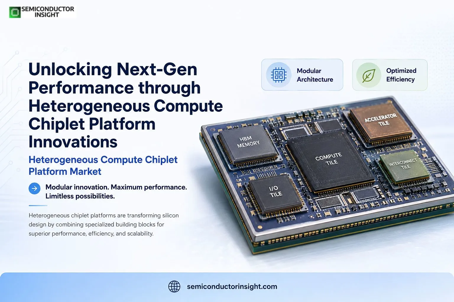
Unlocking Next-Gen Performance through Heterogeneous Compute Chiplet Platform Market Innovations Reshaping Silicon Ecosystems Worldwide
The semiconductor landscape continues evolving rapidly as engineers push beyond traditional monolithic designs. Heterogeneous compute chiplet platforms represent a fundamental shift, breaking complex processors into specialized modular building blocks that connect seamlessly on advanced substrates.
This approach delivers greater flexibility, improved yields, and optimized performance for demanding applications like AI training, high-performance computing, and edge processing.
Evolution from Monolithic Giants to Modular Chiplet Assemblies
- Early semiconductor designs packed everything onto one large silicon die, but physical and economic limits emerged as feature sizes shrank.
- Chiplets emerged as a practical solution, allowing different functional units such as compute cores, memory controllers, or I/O interfaces to be fabricated on their optimal process nodes and later integrated.
- Wikipedia notes that 2.5D integration places multiple dies side-by-side on a silicon interposer, enabling heterogeneous combinations without full 3D stacking complexities.
- This modular philosophy gained traction in commercial products. AMD pioneered high-volume adoption with its EPYC server processors, using multiple chiplets connected via Infinity Fabric to scale core counts efficiently while controlling costs.
- The design separated high-performance cores on advanced nodes from I/O components on more mature processes, demonstrating tangible manufacturing advantages.
Operational Use Cases Shaping Industry Expansion
Intel advanced the concept with its Ponte Vecchio GPU for data centers, integrating diverse chiplets including compute tiles, memory, and interconnects using EMIB and Foveros packaging. This heterogeneous platform tackled extreme performance needs in AI and supercomputing by mixing technologies that would be difficult or expensive on a single die.
TSMC supported these shifts through technologies like CoWoS and SoIC, facilitating high-bandwidth connections between chiplets. Their approach enabled companies to combine logic, memory, and specialized accelerators in single packages, accelerating time-to-market for complex systems. Government initiatives, such as the U.S. CHIPS and Science Act, further bolstered domestic capabilities in advanced packaging and heterogeneous integration, allocating significant funding toward R&D and manufacturing infrastructure.
Performance Gains and Efficiency Breakthroughs in Action
- Chiplet-based systems often achieve better power efficiency and thermal characteristics than monolithic alternatives. By optimizing each tile independently, designers reduce waste and improve overall yields critical when producing large dies prone to defects. Case studies from academic and industry sources show energy-delay product improvements in specialized workloads, sometimes reaching multiples over traditional architectures.
- In high-performance computing, these platforms handle massive parallelism. For instance, configurations supporting transformer models benefit from tailored memory and compute chiplets placed strategically on interposers, minimizing data movement latency. Prototypes and commercial implementations demonstrate scalability across varying model sizes while addressing thermal and power constraints.
For More Detailed Insights, You Can Surf Our Latest Report Here: https://semiconductorinsight.com/report/heterogeneous-compute-chiplet-platform-market/
Interconnect Standards Fuelling Broader Adoption
Standardization efforts like Universal Chiplet Interconnect Express (UCIe) play a vital role in creating an open ecosystem. This specification aims for plug-and-play interoperability, similar to established board-level standards, allowing chiplets from different vendors to integrate reliably. Such frameworks lower barriers for smaller innovators and promote a vibrant marketplace for specialized IP blocks.
Open-source initiatives and research platforms explore heterogeneous computing with chiplets, fostering collaboration across universities and labs. These projects develop frameworks for AI acceleration and edge applications, testing novel memory hierarchies and interconnect fabrics.
Global Collaboration and Supply Chain Dynamics
International partnerships shape progress in this space. Foundries, design houses, and equipment makers coordinate on packaging technologies, from silicon interposers to hybrid bonding methods. Asian manufacturing hubs contribute significantly to volume production, while North American and European entities focus on R&D and specialized applications in defence, automotive, and scientific computing.
Emerging use cases extend beyond traditional computing. Medical imaging systems leverage chiplet integration for AI-powered processing, combining sensor interfaces with acceleration logic in compact, efficient packages. Automotive applications explore modular designs for safety-critical and infotainment functions.
Sustainability and Scalability Considerations
Modular architectures support more sustainable manufacturing by improving yields and enabling reuse of proven chiplet designs across product generations. Instead of redesigning entire SoCs, teams swap or upgrade specific tiles, reducing development resources and material waste. This aligns with broader industry goals around energy efficiency in data centers facing explosive AI-driven demand.
Emerging Frontiers and Integration Pathways
- Research continues into advanced 2.5D and 3D variants, including wafer-scale approaches and novel materials for interconnects.
- Universities and national labs experiment with extremely large integrated circuits built from hundreds of chiplets, targeting applications requiring unprecedented scale.
- The heterogeneous compute chiplet platform market stands at an inflection point.
- As more players adopt these techniques and standards mature, the technology promises to democratize access to cutting-edge performance while addressing economic and technical hurdles of traditional scaling.
Continued investment in packaging, testing, and ecosystem tools will determine how quickly these modular platforms transform computing infrastructure globally.

Comments (0)