

Ultra High Speed Data Pathways and Endurance Optimizations Accelerating PCIe SSD for AI Market in Modern AI Infrastructures
PCIe SSDs have emerged as the essential high-performance storage backbone that keeps AI accelerators fed with massive datasets at the blistering speeds required for training and inference workloads.
These drives connect directly through the PCIe bus to deliver low-latency access that prevents expensive GPU idle time while handling the enormous parallel data streams typical of transformer models and large-scale neural networks. By combining the latest interface standards with purpose-built NAND architectures, manufacturers create solutions that balance extreme throughput, sustained endurance, and efficient power delivery in dense data-center racks.
PCIe Protocol Breakthroughs Delivering Massive Bandwidth for AI Accelerators
- The PCI-SIG has defined clear technical leaps that directly address AI demands through successive generations of the PCIe specification.
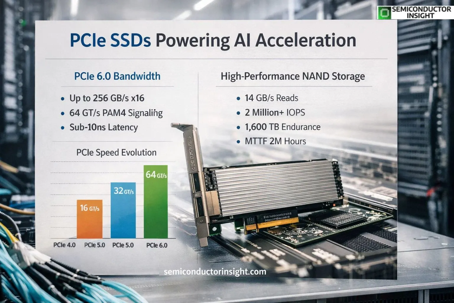
- PCIe 6.0 reaches a raw data rate of 64 GT/s per lane using PAM4 signaling and Flit-based encoding, delivering up to 256 GB/s bidirectional bandwidth in an x16 configuration while maintaining latency additions below 10 nanoseconds even with forward error correction.
- This doubles the 32 GT/s of PCIe 5.0 and preserves full backward compatibility across earlier generations.
- Lightweight FEC combined with strong CRC keeps the bit error rate in check without the heavy overhead seen in networking protocols, ensuring reliable data movement even under continuous high-queue-depth AI workloads.
- Official PCI-SIG documentation highlights how these features scale efficiently for data-intensive markets including artificial intelligence and machine learning clusters.
NAND Architectures Optimized for Continuous AI Training Cycles
Enterprise-grade PCIe SSDs employ advanced TLC and QLC NAND configurations engineered for the write-intensive patterns of AI data pipelines. Typical high-end models achieve sequential read speeds up to 14,500 MB/s and write speeds reaching 12,000 MB/s, with random read IOPS exceeding 2,100K and write IOPS at 2,100K on 4 TB capacities.
Endurance ratings measured in terabytes written (TBW) range from 300 TB for smaller drives to 1,600 TB on higher-capacity units, while mean time to failure (MTTF) consistently hits 2 million hours. Read latency sits at 50 microseconds and write latency at 12 microseconds under typical conditions, figures validated in manufacturer datasheets using standardized IOmeter testing. These metrics allow a single drive to sustain multiple GPU streams without throttling, reducing the total number of SSDs needed in a training node.
Key performance and reliability parameters that AI system designers track include:
- Sequential throughput exceeding 14 GB/s to match GPU memory bandwidth demands
- Random IOPS above 2 million to handle checkpointing and data shuffling
- TBW ratings scaled to support multi-petabyte write volumes over years of continuous operation
- Active power draw under 8,500 mW during peak reads to fit within rack thermal budgets
- MTBF values of 2 million hours ensuring five-nines uptime in hyperscale deployments
To find out more, feel free to browse our latest updated report: https://semiconductorinsight.com/report/pcie-ssd-for-ai-market/
Thermal Design Strategies Maintaining Stability Under Intense AI Compute Loads
AI racks generate extreme localized heat, making thermal management a core semiconductor-level consideration for PCIe SSDs. Newer designs incorporate single-sided printed circuit boards and host-controlled thermal throttling that dynamically adjust performance to stay within safe operating envelopes. Advanced power states such as L0p allow scalable consumption tied directly to bandwidth usage without interrupting traffic flow.
In practice, these features enable liquid-cooling compatibility and reduce overall rack airflow requirements while preserving the sub-10-nanosecond latency budgets critical for real-time inference. Standardized testing protocols confirm that properly engineered drives maintain full specification performance even when ambient temperatures approach the upper limits defined for enterprise environments.
GPUDirect Storage Protocols Streamlining Data Flow from SSD to GPU Memory
- NVIDIA’s GPUDirect Storage technology creates a direct DMA pathway between NVMe PCIe SSDs and GPU memory, bypassing CPU and host DRAM entirely. This eliminates extra data copies that previously consumed valuable cycles and introduced latency spikes during deep-learning training.
- In real implementations, the approach supports high-bandwidth transfers that keep GPU utilization near maximum even when loading terabyte-scale datasets for model training or real-time inference.
- Combined with PCIe 6.0’s 256 GB/s capability, the protocol enables storage disaggregation across RDMA fabrics while preserving near-local latency, a configuration now standard in platforms like the NVIDIA Vera Rubin architecture that pairs Gen6 PCIe with next-generation NVLink interconnects.
These technical advancements in interface standards, NAND endurance, thermal control, and direct GPU integration continue to refine how storage serves the insatiable data appetite of AI systems. Every generation of PCIe SSD brings measurable improvements in bandwidth, latency, and efficiency that translate directly into faster model convergence and lower operational overhead across the world’s most demanding computing environment

Comments (0)