

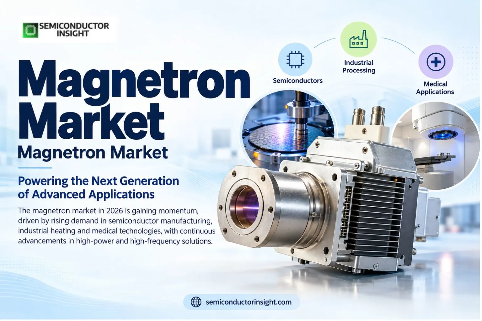
Top 5 Major Leading Regions for magnetron market in 2026 as Semiconductor Thin-Film Engineering, Advanced Coatings and Next-Generation Electronics Reshape Global Demand
Magnetron market in 2026 is closely connected to advances in semiconductor fabrication, precision thin-film deposition, optical coatings, sensors and electronic materials. Magnetrons help generate and sustain plasma in sputtering systems, enabling atoms from a target material to deposit as controlled films on a substrate.
These films can perform essential functions such as electrical conduction, diffusion protection, optical reflection and surface modification. Although magnetron-specific demand is not consistently reported by region in public statistics, semiconductor manufacturing activity, equipment investment and research developments provide useful indicators of where demand opportunities are emerging.
Asia Pacific Turns Semiconductor Scale into a Magnetron Opportunity
Asia Pacific remains a critical region for magnetron technology because of its concentration of semiconductor manufacturing, electronics production and materials research. China installed nearly 370 GW of solar photovoltaic capacity in 2025, while India commissioned almost 50 GW, according to the International Energy Agency. These installations are not direct measures of magnetron sales, but they illustrate the region’s expanding ecosystem for thin-film materials, solar technologies and electronic components.
- Japan and South Korea also contribute through advanced materials engineering, chip fabrication and precision equipment development.
- A September 2025 University of Tsukuba research announcement demonstrated machine-learning-assisted monitoring of iron-oxide thin films during reactive magnetron sputtering, highlighting how process control is becoming increasingly sophisticated.
North America Connects Magnetron Systems with Advanced Chip Manufacturing
North America’s opportunity is supported by semiconductor facility expansion and demand for increasingly complex chip structures. The U.S. Government Accountability Office reported that, as of July 2025, the Department of Commerce had awarded $30.9 billion in direct funding across 40 semiconductor projects. These projects cover facility construction, expansion and modernization, creating a broader environment for deposition equipment and process technologies.
For magnetron suppliers, the relevant applications include conductive films, metal barriers, research-scale materials development and specialised coatings. Procurement decisions depend on film uniformity, target utilisation, contamination control and compatibility with existing vacuum platforms not simply the number of new fabs.
Europe Prioritises Process Precision and Materials Innovation
- Europe combines established semiconductor manufacturers with strong automotive electronics, industrial coatings and scientific research capabilities.
- The European Commission’s Chips Act programme has approved 18 state-aid decisions for first-of-a-kind semiconductor facilities, representing more than €32 billion in public and private investment.
- This activity is relevant to magnetron technology because European manufacturers need dependable deposition processes for power electronics, sensors and specialised components.
- Automotive applications are particularly important: thin films may support electrical contacts, protective layers and functional surfaces.
- Europe’s opportunity therefore lies not only in high-volume chip production but also in specialised manufacturing where precise film properties and process repeatability are essential.
A Brief Look at Our Detailed Analysis Related Report: https://semiconductorinsight.com/report/magnetron-market/
Latin America Builds Opportunity through Solar and Applied Electronics
Latin America presents a different growth profile, with opportunities linked to renewable energy, industrial components, research institutions and local electronics production. Brazil’s expanding digital infrastructure and technology programmes create a foundation for specialised materials development, although publicly available statistics do not isolate regional magnetron installations or sales.
The connection with solar technology is worth monitoring. Global photovoltaic capacity reached nearly 3 TW in 2025, with approximately 698 GW of new systems installed worldwide, according to IEA-PVPS. This expansion supports continued work on functional materials and coatings, but it should not be interpreted as equivalent demand for magnetron equipment because solar technologies use multiple manufacturing processes.
Middle East & Africa Develops Demand through Energy and Industrial Diversification
The Middle East and Africa represent an emerging opportunity for magnetron suppliers as renewable-energy projects, industrial diversification and technical research expand. The IEA reported that renewable capacity additions in both the Middle East and North Africa and sub-Saharan Africa reached approximately 12 GW each in 2025. Saudi Arabia added nearly 7 GW of solar capacity, while South Africa installed more than 3 GW for the first time.
These figures indicate growing activity in energy technologies and related supply chains, rather than measured magnetron demand. Prospects are likely to depend on local manufacturing depth, access to vacuum equipment, technical expertise and partnerships with international deposition-system providers.
Where Magnetron Technology Fits Across the Manufacturing Chain
The manufacturing process begins with target preparation, providing a metal or ceramic target as the material source for sputtering. Plasma generation enables controlled atom ejection, producing a sputtered material flux.
- During thin-film deposition, this material forms functional conductive or protective layers. Finally, process inspection verifies film thickness and quality, resulting in a qualified coated component.
The 2026 Technology Shift Worth Watching
A major development is the effort to move beyond simply depositing a film toward controlling its composition and structure in real time. Research published in 2025 examined machine-learning-based analysis of plasma emission during reactive magnetron sputtering, while another industrial study reported metal-ion fractions reaching up to 30% under the investigated industrial conditions. These findings show why process monitoring, scalable deposition and repeatability are becoming important technical priorities.
The practical pathway is increasingly clear: material selection → plasma control → film deposition → real-time inspection → component qualification. For 2026, this process-led perspective offers a more useful way to understand regional magnetron opportunities than relying on unverified regional sales estimates.

Comments (0)