
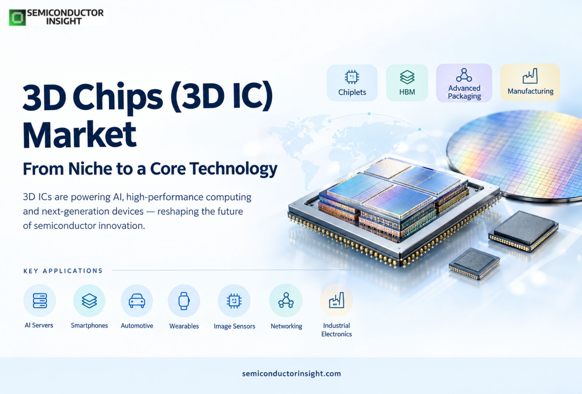
Top 5 Major Leading Regions Shaping the 3D Chips (3D IC) Market in 2026
The 3D Chips (3D IC) market is moving from an advanced-packaging niche into a central technology layer for AI accelerators, high-performance computing, mobile processors, memory systems, automotive electronics and increasingly compact wearable devices.
In 2026, regional momentum is being shaped less by conventional chip volumes and more by access to advanced packaging, semiconductor fabrication capacity, chiplet ecosystems, high-bandwidth memory and large-scale electronics manufacturing.
North America Builds the High-Performance Computing Core
North America remains an important center for 3D IC development because of its concentration of semiconductor designers, AI accelerator companies, hyperscale computing infrastructure and advanced packaging research. The United States is particularly significant for architectures where stacked logic, memory and chiplets are used to increase computing performance.
TSMC’s Arizona expansion is also relevant to the broader U.S. semiconductor ecosystem. The company announced plans involving multiple fabs, advanced packaging facilities and R&D capabilities in Arizona, strengthening the domestic infrastructure available for advanced semiconductor manufacturing.
AI computing is an especially important application. NVIDIA’s Blackwell platform, AMD’s advanced accelerator architectures and high-bandwidth-memory-based AI systems demonstrate the increasing importance of combining multiple dies and advanced packaging techniques rather than depending entirely on conventional single-die processors.
Regional snapshot: AI accelerators → chiplets → HBM → advanced packaging → data-center computing
The region’s influence therefore extends from semiconductor architecture and EDA design through packaging technologies and hyperscale deployment.
Asia Pacific Controls the Manufacturing and Packaging Engine
· Asia Pacific represents the most extensive semiconductor manufacturing ecosystem for 3D IC development. Taiwan, South Korea, Japan and China collectively provide major capabilities spanning foundries, memory, semiconductor equipment, packaging and electronics manufacturing.
· TSMC’s CoWoS and other advanced packaging technologies have become closely associated with AI accelerator production, while Samsung and SK hynix remain major players in advanced memory technologies that complement vertically integrated computing architectures.
· Taiwan is particularly important because TSMC operates one of the world’s largest advanced foundry ecosystems. South Korea contributes enormous memory-manufacturing capacity, with Samsung and SK hynix developing increasingly sophisticated HBM generations for AI systems.
· Japan contributes semiconductor materials, equipment and precision manufacturing. Companies such as Tokyo Electron, SCREEN Semiconductor Solutions and Advantest participate in different stages of the semiconductor production ecosystem.
2026 application map:
AI servers | HBM | smartphones | automotive processors | image sensors | networking | industrial electronics
The region’s strength comes from having multiple parts of the semiconductor value chain located relatively close together.
Europe Strengthens 3D Integration through Automotive and Industrial Chips
Europe’s 3D IC opportunity is closely connected to automotive electronics, industrial automation, power electronics, sensors and specialized computing. Germany, France, Belgium and the Netherlands provide important semiconductor research, manufacturing and equipment capabilities.
imec in Belgium has been particularly influential in advanced semiconductor research, including 3D integration, hybrid bonding and chiplet architectures. The European semiconductor ecosystem also benefits from companies such as ASML, whose lithography systems are fundamental to advanced chip manufacturing worldwide.
The automotive connection is especially important. Modern vehicles can contain hundreds of semiconductor components, while software-defined vehicles require increasing computing capability for sensing, connectivity and automated driving.
Europe’s 3D IC development is therefore increasingly tied to compact, high-reliability computing systems rather than only data-center processors.
Latin America Opens a Specialized Electronics Opportunity
Latin America is not currently comparable with Asia Pacific in semiconductor fabrication scale, but its importance is emerging through electronics manufacturing, automotive production, telecommunications and semiconductor research.
Brazil and Mexico are particularly relevant. Mexico’s position within North American electronics and automotive supply chains creates opportunities for advanced semiconductor packaging and system-level integration. Brazil has also developed semiconductor-related industrial and research capabilities.
The region’s potential applications include automotive electronics, industrial control systems, telecommunications equipment, consumer electronics and IoT devices.
Rather than competing primarily through leading-edge wafer fabrication, Latin America’s opportunity is increasingly connected with downstream semiconductor assembly, testing, electronics integration and regional supply-chain diversification.
Middle East & Africa Develops the Next Semiconductor Demand Layer
The Middle East and Africa represent an emerging rather than mature 3D IC manufacturing region. The strongest opportunity is connected to rapidly expanding digital infrastructure, AI computing, telecommunications, smart-city systems and advanced industrial automation.
Saudi Arabia and the United Arab Emirates are investing heavily in AI infrastructure and digital transformation. These developments can increase demand for high-performance computing hardware, networking equipment and energy-efficient processors where advanced packaging becomes increasingly valuable.
Africa’s opportunity is more strongly connected to telecommunications, mobile devices, and cloud services and data infrastructure. As regional data-center capacity grows, demand for efficient computing and networking hardware can create additional downstream demand for advanced semiconductor architectures.
Curious about the report? Dive into our newest updated version at no cost: https://semiconductorinsight.com/report/global-3d-chips-3d-ic-market/
Wearable Technology Becomes a Compact 3D IC Testbed
Wearables provide an especially interesting application because device manufacturers need more computing capability inside extremely limited physical space.
The International Data Corporation reported that worldwide shipments of wearable devices reached hundreds of millions of units annually, covering smartwatches, wireless earbuds, fitness trackers and other wearable categories. This creates a large installed hardware ecosystem where smaller and more power-efficient semiconductor architectures can provide meaningful advantages.
3D integration can place processing, memory and specialized functions closer together, reducing board-level space requirements. For smartwatches, medical wearables, augmented-reality devices and hearables, this can support more local AI processing while preserving compact form factors.
A typical future wearable architecture can be represented as:
Sensor Layer → AI/Signal Processor → Stacked Memory → Wireless Connectivity → Battery-Efficient Edge Computing
This makes wearables one of the most interesting smaller-form-factor applications for vertically integrated semiconductor architectures.
A New Regional Supply-Chain Pattern
U.S. AI Architecture
↓
Taiwan / South Korea Advanced Manufacturing
↓
Japan and Europe Semiconductor Materials & Equipment
↓
Advanced Packaging and Testing
↓
AI Servers + Smartphones + Vehicles + Wearables
↓
Global Electronics Deployment
This interconnected structure is why the 3D IC market cannot be viewed simply through semiconductor wafer production. Its growth is increasingly determined by the combined availability of design expertise, advanced packaging, memory, manufacturing equipment and end-use electronics.

Comments (0)