

Top 5 Major Leading Regions for Wafer Dicing Services Market in 2026
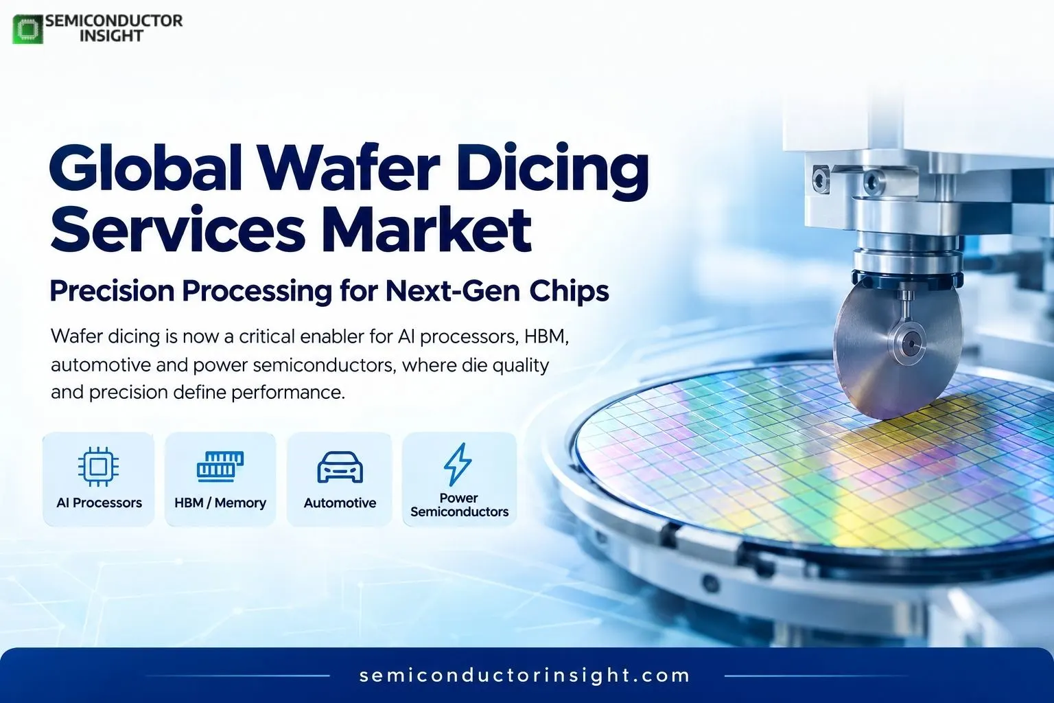
Global wafer dicing is no longer a routine back-end cut. In 2026, it is a precision-control stage for AI processors, HBM, automotive chips, power semiconductors and advanced packaging. As dies become thinner, dicing can influence edge damage, die strength, yield and downstream assembly. SEMI reported worldwide silicon wafer shipments of 3,573 million square inches in Q2 2026, up 7.4% year on year, expanding the wafer base for singulation.
From Cutting Wafers to Controlling Die Quality
Modern wafer dicing services combine blade sawing, laser grooving, stealth dicing, wafer thinning, cleaning, inspection and sorting. DISCO reported in March 2026 that cumulative shipments of its laser saws had exceeded 4,000 units, with shipment pace nearly tripling since 2020. Its newer platforms target low-damage processing for low-k logic, high-density memory and difficult structures.
Wafer fabrication → Thinning → Mounting → Alignment → Blade/Laser Dicing → Cleaning → Inspection → Sorting → Package/Test
Asia Pacific Owns the Production-Density Advantage
- Asia Pacific remains the strongest geography because foundries, memory makers, OSATs and semiconductor equipment suppliers operate in close proximity.
- TSMC reported 15.0 million 12-inch-equivalent wafer shipments in 2025 and more than 17 million wafers of annual manufacturing capacity.
- Its six 12-inch GIGAFAB facilities in Taiwan together exceeded 13 million 12-inch-equivalent wafers of capacity.
- This density supports high-volume dicing and integrated wafer-to-package logistics.
North America Turns Localization into Back-End Opportunity
North America is strengthening its position as new fabrication and packaging capacity moves closer to domestic customers. Intel lists 15 wafer fabs in production worldwide across 10 locations, including Arizona, New Mexico and Oregon in the United States.
Amkor’s Arizona advanced packaging and test project has expanded to a planned $7 billion investment across two phases. Such projects increase demand for regional die preparation, singulation and inspection.
You can freely browse our most recent updated report to learn more about it before scrolling further: https://semiconductorinsight.com/report/wafer-dicing-services-market/
Europe Builds around Precision-Heavy Applications
Europe’s wafer dicing opportunity is strongly connected to automotive, industrial, power and sensor applications. TSMC’s Dresden project is planned around 28/22 nm and 16/12 nm technologies for automotive and industrial products.
Meanwhile, the UK’s 2026 semiconductor study identified 705 semiconductor companies and approximately 16,350 direct employees in dedicated semiconductor firms in 2025.
Latin America Gains through Electronics and Assembly Links
Latin America is smaller in wafer fabrication but is developing useful semiconductor and electronics capabilities. Brazil’s CEITEC remains part of the country’s public semiconductor infrastructure, while Mexico and Costa Rica are connected to electronics, assembly and test supply chains. The opportunity is strongest in outsourced processing, prototyping and smaller production programs for automotive electronics and industrial systems.
Middle East & Africa Carve Out Specialized Niches
- The Middle East & Africa remain smaller production centers, but semiconductor design, research, electronics localization and technology investment are creating selective demand.
- Israel already has established semiconductor manufacturing activity, while Gulf economies are building advanced technology ecosystems.
- Dicing providers can target high-value work in sensors, photonics, power electronics and specialized electronics, where traceability can matter more than scale.
A Quick 2026 Technology Map
Our semiconductor dicing and inspection services are designed to support a broad range of device types and production requirements. Blade dicing is ideal for high-volume silicon wafer singulation, while laser dicing enables low-damage processing for delicate wafers and complex structures. For hard-material power devices, including silicon carbide (SiC) and gallium nitride (GaN), specialised dicing methods ensure reliable and precise results.
The Material Mix Is Changing the Service Equation
Customers are increasingly asking for a controlled die-separation outcome rather than a simple cut. Thin silicon, SiC, GaAs, low-k structures and advanced memory can require different kerf widths, cutting speeds, cooling methods and inspection routines. DISCO’s 2026 technical-review program includes GaAs wafer dicing and SiC dicing technologies, illustrating how material diversity is reshaping process engineering.

Comments (0)