

Top 5 Major Leading Regions for the Advanced Process Photomask Market as High-NA EUV and Sub-2nm Chipmaking Redefine Lithography in 2026
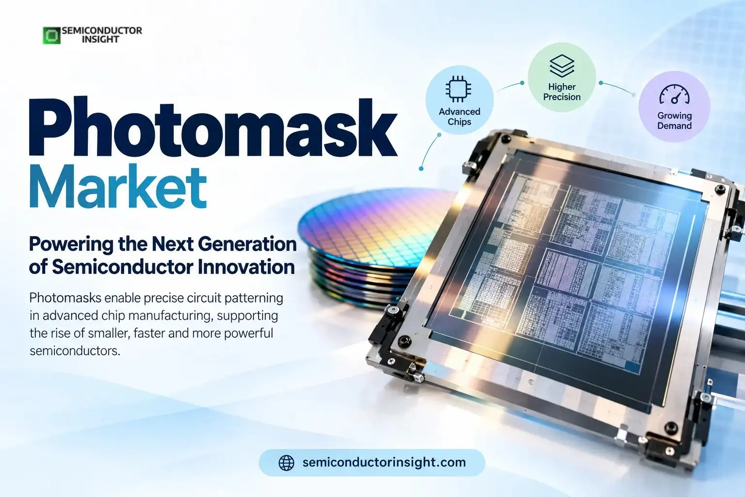
A photomask may look like a relatively small part of semiconductor production, but at advanced nodes it becomes one of the most demanding precision elements in the entire fabrication sequence. It carries the pattern that lithography systems transfer onto a wafer, meaning defects, dimensional errors and pattern-placement problems can ultimately affect thousands of individual dies.
The importance of advanced masks is rising with High-NA EUV. In September 2026, ASML and TSMC announced an industry initiative to develop 12-inch photomasks for High-NA EUV, targeting a pilot line by 2031 and full lithography-system readiness for advanced-node production by 2033. The industry currently relies on 6-inch photomasks for EUV.
Asia Pacific Turns Advanced Mask Manufacturing into a Node-Level Advantage
Asia Pacific remains the most concentrated region for advanced semiconductor manufacturing. SEMI estimates that China will reach approximately 2.4 million 300mm wafers per month in 2026, equivalent to 25% of global 300mm front-end capacity, while Korea is projected at 23% and Taiwan at 21%. Japan is expected to account for about 12%.
- For photomasks, the region’s importance is even more visible through the Taiwan–Korea technology corridor. TSMC entered high-volume manufacturing of its 2nm process in the fourth quarter of 2025 and scheduled N2P and A16 volume production for the second half of 2026.
- Samsung is also joining the 12-inch High-NA EUV photomask initiative and plans to apply High-NA EUV to future DRAM manufacturing.
North America Builds a Domestic Mask-Ready Advanced Fab Ecosystem
North America is changing from a major semiconductor consumer and design center into a larger advanced manufacturing base. TSMC Arizona’s first fab entered high-volume N4 production in the fourth quarter of 2024, while its second fab targets N3 production in the second half of 2027 and its third fab is planned for N2 and A16 technology. Construction of a fourth fab and the first advanced-packaging fab began in early 2026.
The photomask opportunity follows this expansion because every additional advanced lithography layer requires tightly controlled mask preparation, inspection and repair capabilities. Micron’s U.S. expansion is another important signal, with planned facilities in Idaho and New York supporting advanced DRAM and HBM-related production. The U.S. Department of Commerce says the broader Micron program is expected to create around 90,000 jobs.
Europe Strengthens the Research-to-Mask Technology Pipeline
Europe’s influence comes through lithography equipment, research infrastructure and process development. In February 2026, the European Commission announced the opening of NanoIC at imec Leuven, supported by €700 million in EU funding within a €2.5 billion facility investment. The pilot line is Europe’s first facility to deploy the most advanced EUV lithography equipment and focuses on technology beyond 2nm.
This matters to photomask suppliers because advanced research facilities provide the environment where new mask materials, pattern strategies, inspection methods and lithography processes can be validated before industrial deployment. Europe’s Chips Act 2.0 proposal in June 2026 also aims to strengthen advanced semiconductor production and reduce strategic dependencies.
Don’t Forget to Surf Our Updated Report for More Detailed Analysis: https://semiconductorinsight.com/report/advanced-process-photomask-market/
Latin America Moves Upstream Through Semiconductor Design and Electronics Infrastructure
Latin America’s role is developing differently. Mexico recorded 527 economic units in semiconductor and electronic-component manufacturing in May 2026, with Baja California accounting for 112, Sonora 62 and Jalisco 60. Mexico and the United States also held their seventh bilateral semiconductor forum in July 2026 to strengthen investment, industry and academic cooperation.
Brazil is simultaneously strengthening its domestic semiconductor chain through Brasil Semicon, a federal program covering production, research, innovation and chip development. These activities do not yet make Latin America a leading photomask manufacturing center, but they expand the downstream engineering ecosystem that can eventually support semiconductor design, packaging, testing and specialized lithography requirements.
Middle East and Africa Create a New Design and Talent Layer
The Middle East and Africa are building semiconductor capabilities primarily through design, research, education and technology infrastructure. Saudi Arabia’s 2026 Chipathon attracted more than 1,000 students from over 40 universities, with 50 finalists developing projects focused on chip design, memory and embedded-system performance. The winning project involved high-speed, low-power SRAM for in-memory computing and edge AI.
Dubai Silicon Oasis also launched expansion projects totaling AED12.8 billion in January 2026, reinforcing the region’s broader technology and innovation infrastructure. These developments create a growing ecosystem for semiconductor design and advanced electronics, even though high-volume photomask fabrication remains concentrated elsewhere.

Comments (0)