

Top 5 High-Impact Geographic Markets Fuelling Worldwide Adoption of Advanced Line Scan Camera Systems
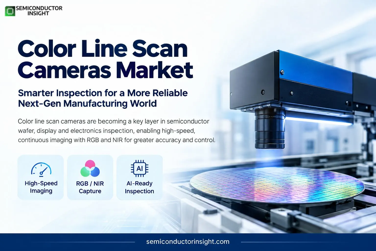
Color line scan cameras are moving from a specialist machine-vision component to an important inspection layer for semiconductor wafers, displays, PCBs, batteries, printed electronics, films and other continuously moving surfaces. Line scan systems are especially useful for high-speed web and wafer inspection because they construct an image one line at a time, as opposed to area-scan cameras that record entire frames. In 2026, commercially available systems already span 2K, 4K, 8K and 16K resolutions, with advanced models reaching line rates of 300 kHz and supporting RGB, RGB+NIR and multispectral imaging. Teledyne, for example, lists 16K color models operating at up to 300 kHz and semiconductor-wafer inspection as an application.
The wider semiconductor ecosystem is providing a strong installation base. Global semiconductor sales reached $795.6 billion in 2025, while the first quarter of 2026 recorded $298.5 billion in sales, according to industry bodies using WSTS data.
A 2026 Inspection Chain Built Around Continuous Imaging
Wafer or material → precision lighting → RGB/NIR line capture → defect detection → image processing → classification → production decision
The attraction is simple: one continuous production surface can be inspected without repeatedly stopping the manufacturing process. Color information also adds another layer of discrimination, helping systems distinguish contamination, coating variation, scratches, stains, pattern differences and material inconsistencies.
North America Holds a High-Value Position through Advanced Inspection Deployment
- North America remains one of the most important regions because semiconductor manufacturing is being rebuilt alongside substantial investment in advanced fabrication, packaging, materials and equipment. In 2026, the Americas are projected to account for nearly 9% of global 300mm front-end fab capacity, up from 2022 levels.
- The United States also generated $425 billion in semiconductor sales through U.S.-headquartered companies in 2025 and recorded $76.8 billion in semiconductor R&D expenditure. More than 160 semiconductor-related projects had been announced across 30 states since 2020, representing more than $770 billion in private-sector investment.
- For color line scan cameras, this creates demand around wafer inspection, advanced packaging, PCB production, display manufacturing and automated quality-control systems. The region’s emphasis is less about simply installing cameras and more about integrating high-resolution imaging with AI-assisted defect classification and real-time manufacturing software.
Europe Strengthens Its Position through Automotive and Industrial Semiconductor Expansion
Europe’s importance is closely connected with automotive electronics, industrial automation, power semiconductors and specialized manufacturing. The European Chips Act targets a 20% share of global semiconductor production by 2030, while the European Commission identified four projects in 2025 as Integrated Production Facilities or Open EU Foundries.
This expansion creates inspection opportunities extending beyond wafer fabrication. Color line scan cameras can examine semiconductor packages, ceramic substrates, PCB surfaces, coated materials and automotive electronic components where even small visual differences can signal manufacturing problems.
Regional signal for 2026: Europe and the Middle East are forecast to record particularly strong semiconductor-fab investment growth in 2026, increasing the potential installation base for automated inspection equipment.
Don’t Forget to Surf Our Updated Report for More Detailed Analysis: https://semiconductorinsight.com/report/color-line-scan-cameras-market/
Asia Pacific Remains the Core Manufacturing Engine
- Asia Pacific is the clear center of gravity because Taiwan, South Korea, Japan, China and Southeast Asia collectively host enormous semiconductor manufacturing capacity. China alone is expected to reach approximately 2.4 million 300mm wafers per month in 2026, representing about 25% of worldwide 300mm front-end fab capacity.
- Taiwan is equally significant. TSMC reported more than 17 million 12-inch-equivalent wafers of annual capacity in 2025, with manufacturing spread across Taiwan and overseas facilities in China, the United States and Japan. The company manufactured 12,682 products for 534 customers using 305 distinct process technologies during 2025.
- This density of production makes Asia Pacific the strongest deployment environment for color line scan cameras. Inspection extends across wafers, masks, packaging, PCBs, displays, batteries and semiconductor materials. High-speed multiline cameras are especially valuable where RGB and NIR information must be collected during a single production pass.
Latin America Is Building a Smaller but More Strategic Inspection Base
Latin America’s role is developing around electronics assembly, semiconductor design, testing, industrial automation and localized technology programs rather than the scale of East Asian wafer fabrication. Brazil is particularly important. Its Brasil Semicon program, established under the country’s semiconductor legislation, is designed to strengthen chip production, research, innovation and electronic-component capabilities.
Brazil’s government reported more than R$1.2 billion in semiconductor-related fiscal incentives between 2020 and 2025 and planned more than R$1.2 billion in FNDCT funding for semiconductor activities in 2026. It also reported training approximately 1,860 semiconductor professionals, with a target of 4,000 additional engineers and designers by 2028.
For camera suppliers, this creates a gradual opportunity in chip testing, electronics inspection, packaging, identification systems and advanced industrial vision.
Middle East and Africa Emerging Through New Semiconductor Infrastructure
The Middle East and Africa currently represent a smaller installed base for semiconductor manufacturing cameras, but their strategic importance is increasing as governments seek domestic technology capabilities and advanced industrial infrastructure. Semiconductor capacity forecasts group Europe and the Middle East together at around 7% of global 300mm front-end capacity in 2026, up from 6% in 2022.
The region’s opportunity is therefore closely tied to new fabs, electronics assembly, defense technology, renewable-energy electronics and automated industrial inspection. As production environments become more automated, color imaging can provide an additional quality-control layer for components where surface condition and spectral differences matter.
What Is Changing Inside the Camera?
The next competitive shift is not simply higher resolution. Multispectral sensing, NIR capability, HDR, fiber connectivity, Camera Link HS and 5GigE interfaces are becoming increasingly relevant. A current 5GigE color line scan platform can deliver 500 MB/s bandwidth, while newer multispectral architectures combine RGB and NIR capture in one scanning system.
Another notable development is integrated contact-image sensing. Teledyne’s color AxCIS platform combines sensor, optics and lighting and can operate at up to 60 kHz × 3 RGB line rates at 28 µm pixel size, illustrating how inspection hardware is being packaged into more compact production-ready systems.

Comments (0)