
Semiconductor Wafer Dicing Blade Market Insights
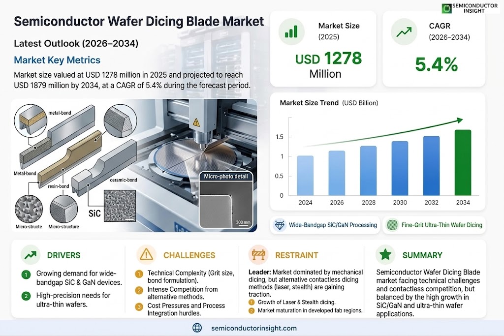
Global Semiconductor Wafer Dicing Blade market size was valued at USD 1.28 billion in 2025. The market is projected to grow from USD 1.35 billion in 2026 to USD 1.88 billion by 2034, exhibiting a CAGR of 5.4% during the forecast period.
A Semiconductor Wafer Dicing Blade is a high-precision consumable tool designed for the singulation, or dicing, of semiconductor wafers into individual chips or dies. These blades are critical components in the backend manufacturing process, where they perform mechanical cutting through materials like silicon, gallium arsenide, and silicon carbide using ultra-thin, diamond-embedded edges mounted on a rotating spindle. The primary function is to achieve clean, precise cuts with minimal chipping and kerf loss to maximize die yield from each wafer.
The market growth is primarily driven by the relentless expansion of Global semiconductor industry and the increasing complexity of device packaging. Key demand drivers include the proliferation of 5G infrastructure, artificial intelligence (AI) hardware, and high-performance computing (HPC), all of which require advanced nodes and heterogeneous integration that push dicing precision to its limits. Furthermore, the rise of wide-bandgap semiconductors for electric vehicles and renewable energy applications necessitates blades capable of cutting harder materials like silicon carbide (SiC) and gallium nitride (GaN). However, the market faces challenges from alternative singulation technologies such as stealth dicing and laser ablation, which are gaining traction for ultra-thin wafers. Leading players like DISCO Corporation and Tokyo Seimitsu Co., Ltd. dominate this highly technical segment through continuous innovation in blade metallurgy and diamond grit technology to improve cut quality and tool life.
MARKET DRIVERS
Proliferation of Advanced Semiconductor Packaging
The relentless push toward miniaturization and enhanced performance in electronics is a primary driver for the Semiconductor Wafer Dicing Blade Market. The rise of advanced packaging technologies, such as fan-out wafer-level packaging (FO-WLP), 3D IC integration, and system-in-package (SiP), demands exceptionally precise and clean dicing processes. These technologies handle thinner, more fragile wafers and utilize materials like silicon, glass, and compound semiconductors (e.g., GaN, SiC), all of which require specialized dicing blades to prevent chipping, cracking, and delamination, thereby sustaining market growth.
Expansion of Automotive and Industrial Electronics
The automotive sector’s rapid electrification and adoption of ADAS (Advanced Driver-Assistance Systems), alongside increasing automation in industrial applications, are creating robust demand for power semiconductors and sensors. These components, often built on robust but difficult-to-process materials like silicon carbide (SiC) for electric vehicle inverters, necessitate the use of high-performance, durable, diamond-embedded dicing blades. This sector’s growth directly correlates with increased consumption within the Semiconductor Wafer Dicing Blade Market.
➤ Global demand for more connected devices and IoT sensors continues to place immense pressure on semiconductor manufacturing capacity, directly translating to higher volumes of wafer dicing operations and, consequently, steady demand for both standard and specialized dicing blades.
Furthermore, sustained investment in semiconductor fabrication capacity globally, including the establishment of new foundries and the expansion of existing ones, provides a foundational driver for all associated equipment and consumables, including the critical Semiconductor Wafer Dicing Blade Market.
MARKET CHALLENGES
Technical and Material Complexity in Dicing
The semiconductor industry’s evolution presents significant technical challenges for the Semiconductor Wafer Dicing Blade Market. Dicing ultra-thin wafers (below 100µm) for advanced memory and logic chips, as well as processing hard, brittle compound semiconductor materials, requires blades with extremely fine grit sizes and specialized bond formulations. Achieving the necessary kerf quality (cut width) and cut-edge integrity without introducing micro-cracks or contamination is a persistent engineering hurdle that increases R&D and production costs for blade manufacturers.
Other Challenges
Cost Pressure and Intense Competition
Manufacturers in the Semiconductor Wafer Dicing Blade Market operate under constant cost pressure from semiconductor device makers seeking to lower production expenses. This is compounded by intense competition among blade suppliers, which can erode profit margins. The need for continuous innovation to support next-generation materials and processes further strains profitability, creating a challenging environment that demands high operational efficiency.
Process Integration and Tool Compatibility
Integrating new, advanced dicing blade technologies into existing high-volume manufacturing lines poses a significant challenge. Any change in blade specification must be rigorously validated to ensure compatibility with dicing saws from various OEMs and to maintain throughput and yield. This validation process is time-consuming and costly, potentially slowing the adoption of innovative blade solutions in established fabs.
MARKET RESTRAINTS
Alternative Dicing Technologies Gaining Traction
A key restraint on the traditional Semiconductor Wafer Dicing Blade Market is the growing adoption of alternative singulation methods, particularly laser dicing and stealth dicing. For certain applications, such as processing very thin wafers or devices highly sensitive to mechanical stress, these contactless technologies offer advantages like no blade wear, reduced chipping, and the ability to perform intricate street patterns. While mechanical dicing remains dominant for most materials, this competitive pressure constrains market growth potential in specific high-value segments.
Cyclical Nature of Semiconductor Capital Expenditure
The market’s growth is inherently tied to the capital expenditure (CapEx) cycles of the broader semiconductor industry. During periods of downturn or reduced equipment investment, demand for consumables like dicing blades can soften as fabs optimize existing blade inventories and extend blade life. This cyclicality introduces an element of volatility and forecasting difficulty for participants in the Semiconductor Wafer Dicing Blade Market, restraining steady, linear growth.
MARKET OPPORTUNITIES
Wide-Bandgap Semiconductor Material Processing
The accelerating adoption of silicon carbide (SiC) and gallium nitride (GaN) for power electronics and RF devices represents a substantial opportunity for the Semiconductor Wafer Dicing Blade Market. These hard, brittle materials are exceptionally challenging to dice cleanly. Developing and supplying specialized blades—such as ultra-fine diamond blades or blades with novel metal/resin hybrid bonds optimized for these substrates—allows manufacturers to capture value in this fast-growing, high-margin niche, securing a strategic position in next-generation semiconductor manufacturing.
Innovation in Blade Technology and Services
Opportunities abound in technological innovation and service-oriented business models. Developing blades with engineered abrasives, advanced cooling channels for high-speed dicing, or coatings that reduce debris adhesion can deliver superior performance. Furthermore, offering predictive maintenance services, blade life monitoring through IoT sensors, and customized blade reconditioning programs can create recurring revenue streams and deepen customer relationships within the Semiconductor Wafer Dicing Blade Market, shifting the dynamic from a pure product sale to a solutions partnership.
Expansion in Emerging Fab Clusters
Global push for geographic diversification of semiconductor supply chains, leading to the construction of new fabrication facilities in regions like North America, Europe, and Southeast Asia, presents a clear expansion opportunity. Establishing a strong local supply chain presence, including technical support and inventory hubs, near these emerging fab clusters will be crucial for blade manufacturers to capture new demand from greenfield facilities and gain market share from established regional incumbents.
Key Semiconductor Wafer Dicing Blade Market Trends
Precision Demands Drive Advanced Blade Technology
The relentless push for miniaturization and higher performance in semiconductor devices is a primary driver of trends in the Semiconductor Wafer Dicing Blade Market. As integrated circuits become smaller and more complex, the demand for unprecedented cutting precision intensifies. This is leading to accelerated adoption of newer, more sophisticated blade technologies. Laser-assisted cutting systems, which reduce mechanical stress and minimize chipping, are gaining significant traction. Concurrently, innovations in diamond-coated blade technology are being widely implemented to enhance blade longevity and cutting efficiency, directly addressing the need for cost-effective, high-yield production processes.
Other Trends
Downstream Demand from 5G, AI, and EVs
Demand dynamics within the Semiconductor Wafer Dicing Blade Market are being reshaped by key downstream industries. The extensive commercialization of 5G infrastructure, the proliferation of artificial intelligence hardware, and the electrification of the automotive sector are creating sustained demand for advanced microelectronic components. This directly translates into a need for high-precision dicing blades capable of handling diverse and challenging materials, from traditional silicon to advanced compound semiconductors used in power electronics and optoelectronic devices like LEDs and sensors.
Market Consolidation and Competitive Innovation
The competitive landscape of the Semiconductor Wafer Dicing Blade Market features a high concentration among established global leaders, yet is simultaneously energized by focused innovation. Dominant players maintain significant shares through technological depth and extensive product portfolios. However, the market also shows a trend where mid-sized and specialized suppliers are capturing niches through product differentiation and rapid adaptation to new material requirements. This environment fosters continuous R&D investment, particularly in smart dicing systems that feature intelligent tool monitoring and automated parameter adjustment, aiming to improve yield and reduce operational downtime for manufacturers.
COMPETITIVE LANDSCAPE
Key Industry Players
A high-concentration market led by precision engineering leaders
Global Semiconductor Wafer Dicing Blade market is characterized by a high degree of concentration, with technological superiority and manufacturing scale being primary competitive differentiators. Japanese manufacturing leader DISCO Corporation is the undisputed market leader, renowned for its comprehensive solutions encompassing dicing blades, saws, and grinders. Alongside other major Japanese players like Asahi Diamond Industrial and Tokyo Seimitsu, these entities command significant market share due to their extensive R&D investment, proven reliability in high-volume manufacturing, and deep integration with semiconductor fabrication processes. The competitive pressure in this tier is intense, focusing on advancements in diamond bonding technology and blade longevity to meet the exacting demands of leading-edge nodes for 300mm wafers.
Beyond the top-tier incumbents, a dynamic ecosystem of specialized and regional players competes vigorously in niche segments and specific applications. Companies such as Kulicke & Soffa Industries leverage their strength in semiconductor packaging equipment, while material science giants like Saint-Gobain and 3M apply their abrasives expertise. Several key manufacturers from China, including Shanghai Sinyang, Xiamen Tungsten, and Nanjing Sanchao Advanced Materials, are expanding their presence, often competing on cost-effectiveness and responsiveness for mature-node wafers (e.g., 200mm) and applications in LEDs, power devices, and optoelectronics. This diverse landscape sees competition through product differentiation in hub versus hubless blade designs, application-specific formulations for advanced compound semiconductors, and value-added services.
List of Key Semiconductor Wafer Dicing Blade Companies Profiled
- DISCO Corporation
- Asahi Diamond Industrial Co., Ltd.
- Kulicke & Soffa Industries, Inc.
- Tokyo Seimitsu Co., Ltd. (ACCRETECH)
- Saint-Gobain S.A.
- 3M Company
- Kinik Company
- UKAM Industrial Superhard Tools
- Shanghai Sinyang Semiconductor Materials Co., Ltd.
- Xiamen Tungsten Co., Ltd.
- Nanjing Sanchao Advanced Materials Co., Ltd.
- Thermocarbon, Inc.
- Ceiba Technologies
- Sungold Abrasives Co., Ltd.
- System Technology Inc.
Segment Analysis:
| Segment Category | Sub-Segments | Key Insights |
| By Type |
|
Hubless Dicing Blades are a dominant innovation, driven by their superior design for chip miniaturization and high-density wafer cutting. The blade’s inherent stability and precision during high-speed cutting for advanced nodes have led to high adoption in cutting-edge semiconductor fabs. These blades minimize vibration and debris generation, which is critical for defect-sensitive processes, thereby delivering enhanced yield and operational consistency for manufacturers of leading-edge integrated circuits. |
| By Application |
|
300mm Wafer applications represent the technology frontier, commanding the highest demand for precision dicing solutions. This leadership is firmly tied to the shift in high-volume manufacturing towards larger wafers for economies of scale in producing logic, memory, and advanced packaging chips. The blades for this segment require exceptional rigidity and edge retention to handle the full diameter and complex material stacks, driving continuous R&D in diamond coatings and laser-assisted cutting technologies to meet stringent throughput and quality requirements. |
| By End User |
|
Semiconductor Manufacturers are the primary and most demanding end-user segment, characterized by an unrelenting pursuit of yield and precision. Their dominance is fueled by the pervasive demand for microelectronics across 5G, AI, automotive, and consumer devices, requiring increasingly complex die singulation. This segment pushes suppliers for blades with extended operational life, compatibility with new brittle materials, and integration into fully automated dicing saws, making it the core driver of technological advancements and premium product development in the market. |
| By Material Technology |
|
Diamond-Based Blades are the undisputed technology leader, essential for cutting hard and brittle semiconductor materials like silicon, silicon carbide, and gallium nitride. Their superior hardness and wear resistance translate directly to consistent cut quality, kerf control, and reduced wafer chipping. The ongoing trend towards harder substrate materials for power electronics and RF devices further cements their dominance, with innovations focusing on optimizing diamond grit size, bond matrix, and the integration of nano-coatings to enhance performance and tool life in high-volume production environments. |
| By Cutting Precision |
|
Ultra-High Precision Singulation is the critical and fastest-evolving segment, driven by the relentless miniaturization of chip features and the advent of advanced packaging like fan-out wafer-level packaging and 3D integration. This segment demands blades capable of producing extremely narrow, clean, and street-free cuts on wafers thinned to near 100 micrometers or less. Success here hinges on minimizing mechanical stress and micro-cracks, which has spurred the convergence of blade technology with in-process monitoring systems and laser hybrid processes to achieve the defect densities required for next-generation electronic products. |
Regional Analysis: Global Semiconductor Wafer Dicing Blade Market
Asia-Pacific
The region’s supremacy is rooted in its dense network of leading-edge fabs and major OSAT companies. This concentration necessitates a continuous, high-volume supply of reliable Semiconductor Wafer Dicing Blade Market consumables, making the region both the largest consumer and producer of these critical tools, driving economies of scale and localized innovation cycles.
A mature, localized ecosystem for high-precision engineering materials like diamonds and resins supports local blade manufacturing. This integration reduces lead times, enhances collaboration between blade developers and wafer fabs, and provides significant cost advantages, underpinning regional competitiveness in Global dicing blade landscape.
Leadership in producing advanced chips for smartphones, AI, and automotive applications forces local manufacturers to pioneer next-generation dicing technologies. This drives demand for blades capable of handling ultra-thin silicon, silicon carbide (SiC), and gallium nitride (GaN) wafers with minimal kerf loss and damage.
The market is characterized by fierce competition between multinational corporations with advanced material science expertise and nimble regional players specializing in cost-optimized solutions. This dynamic pressures all participants to continuously improve blade longevity, cutting speed, and die yield for their customers.
North America
North America holds a position of significant influence in the Semiconductor Wafer Dicing Blade Market, primarily driven by its leadership in semiconductor design, R&D, and the production of high-value, low-volume specialty chips. The region’s market is characterized by demand for ultra-high-precision dicing blades required for cutting-edge applications in aerospace, defense, and high-performance computing. The presence of major fabless design companies and advanced packaging research institutions creates a demand pull for innovative dicing solutions that maximize die integrity for complex, multi-die packages. This focus on quality and performance over pure volume shapes a market where technical partnerships between blade suppliers and manufacturers are crucial for developing application-specific solutions.
Europe
The European market for semiconductor wafer dicing blades is defined by its strong automotive and industrial semiconductor base. Stringent quality and reliability standards in these sectors translate to a demand for highly consistent and durable dicing blades that ensure superior edge quality and minimal micro-cracking. The market is also influenced by significant R&D activities in power electronics, particularly for silicon carbide (SiC) and gallium nitride (GaN) devices used in electric vehicles and renewable energy systems. This drives specialized demand for blades engineered to handle these hard, brittle compound materials effectively, positioning Europe as a key region for specialty and high-reliability segments of the dicing blade market.
South America
South America represents an emerging market for semiconductor wafer dicing blades, with its dynamics largely tied to regional electronics assembly and growing industrial automation. While not a major hub for front-end semiconductor fabrication, the region hosts backend assembly and test operations that consume dicing blades. Market growth is gradual, fueled by increasing local manufacturing of consumer electronics and automotive components. The regional market tends to prioritize cost-effective and reliable blade solutions for established process technologies, with demand influenced by foreign direct investment in electronics manufacturing and the overall expansion of the region’s industrial base.
Middle East & Africa
The Middle East & Africa region currently represents a smaller, developing segment of Global Semiconductor Wafer Dicing Blade Market. Primary demand stems from electronics maintenance, repair, and small-scale assembly operations rather than high-volume wafer production. However, strategic investments in technology and diversification efforts, particularly in Gulf nations to build knowledge-based economies, could gradually introduce downstream semiconductor packaging activities. The regional market dynamics are thus characterized by nascent demand, with a focus on imported, versatile blade products for diverse, lower-volume cutting applications across various industries.
Report Scope
This market research report provides a comprehensive analysis of the Semiconductor Wafer Dicing Blade Market, covering the forecast period 2026–2034. It offers detailed insights into market dynamics, technological advancements, competitive landscape, and key trends shaping the industry.
Key focus areas of the report include:
- Market Overview: The report begins with an overview outlining its current market scenario, key growth indicators, and industry transformation drivers. It discusses macroeconomic factors, demand–supply balance, regulatory landscape, and the strategic role of semiconductors in powering advancements across industries such as automotive, telecommunications, consumer electronics, and industrial automation.
- Market Size & Forecast: Historical data and future projections for revenue, unit shipments, and market value across major regions and segments.
- Segmentation Analysis: Detailed breakdown by product type, technology, application, and end-user industry to identify high-growth segments and investment opportunities.
- Regional Insights: Insights into market performance across North America, Europe, Asia-Pacific, Latin America, and the Middle East & Africa, including country-level analysis where relevant.
- Competitive Landscape: Profiles of leading market participants, including their product offerings, R&D focus, manufacturing capacity, pricing strategies, and recent developments such as mergers, acquisitions, and partnerships.
- Technology Trends & Innovation: Assessment of emerging technologies, integration of AI/IoT, semiconductor design trends, fabrication techniques, and evolving industry standards.
- Market Drivers & Restraints: Evaluation of factors driving market growth along with challenges, supply chain constraints, regulatory issues, and market-entry barriers.
- Stakeholder Insights: Insights for component suppliers, OEMs, system integrators, investors, and policymakers regarding the evolving ecosystem and strategic opportunities.
Primary and secondary research methods are employed, including interviews with industry experts, data from verified sources, and real-time market intelligence to ensure the accuracy and reliability of the insights presented.
FREQUENTLY ASKED QUESTIONS:
What is the current market size of Semiconductor Wafer Dicing Blade Market?
-> Global Semiconductor Wafer Dicing Blade market was valued at USD 1278 million in 2025 and is projected to reach USD 1879 million by 2034, at a CAGR of 5.4% during the forecast period.
Which key companies operate in Semiconductor Wafer Dicing Blade Market?
-> Key players include DISCO Corporation, Mitsubishi Heavy Industries, Asahi Diamond Industrial, Kulicke & Soffa Industries, UKAM, Ceiba, and Shanghai Sinyang, among others. The market is relatively concentrated with leading global players holding significant share.
What are the key growth drivers?
-> Key growth drivers include Global expansion of semiconductor, consumer electronics, and optoelectronic industries, driven by technologies like 5G, AI, and IoT. Increasing adoption of electric vehicles, solar energy, and smart devices, alongside the trend of product miniaturization, further boosts demand for high-precision dicing blades.
Which region dominates the market?
-> The report provides detailed regional analysis. High growth is driven by downstream semiconductor and electronics manufacturing, with Asia being a key region including major markets like China, Japan, and South Korea.
What are the emerging trends?
-> Emerging trends include the wider adoption of laser-assisted cutting technology and diamond-coated blade technology to enhance efficiency and blade lifespan. Future trends point towards smart and automated dicing equipment with intelligent tool monitoring and automated parameter adjustment.

Get Sample Report PDF for Exclusive Insights
Report Sample Includes
- Table of Contents
- List of Tables & Figures
- Charts, Research Methodology, and more...
 Download Sample Report PDF





