

Top 15 Leading Manufacturers and Suppliers Transforming the Global Test Grade Wafers Industry
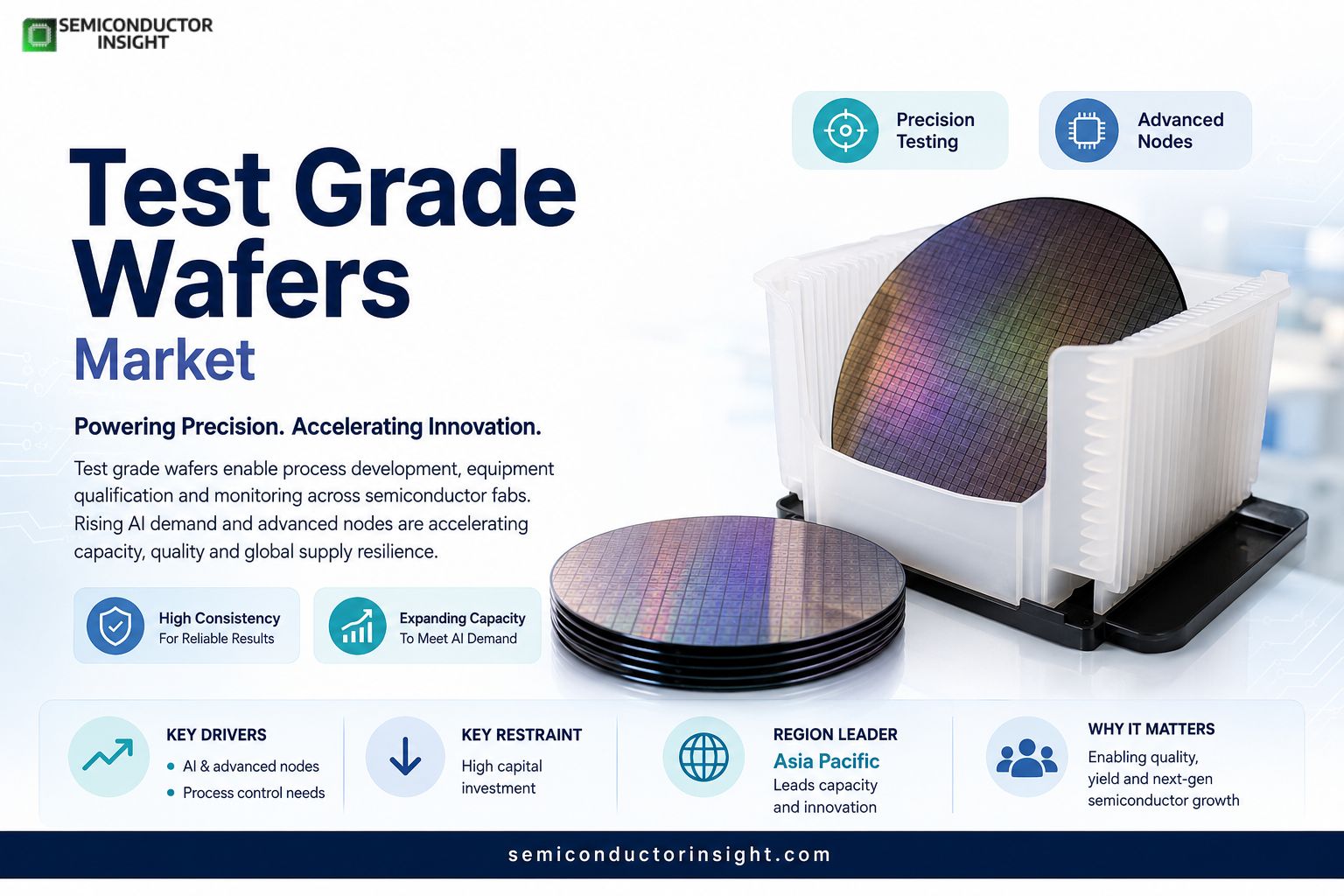
Test Grade Wafers Market refers to the industry involved in producing and supplying silicon and other semiconductor wafers specifically designed for process development, equipment qualification, calibration, process monitoring, research, and non-production testing in semiconductor manufacturing.
Shin-Etsu Chemical
Japan’s long-standing powerhouse in semiconductor silicon has anchored the industry since its early mass production of 300 mm wafers at the Shirakawa Plant in 2001. With roughly 27,300 employees across operations in 17 countries as of late 2025 and early 2026 figures, the company sustains one of the world’s largest wafer outputs. Its electronics materials division ships polished, epitaxial, and related wafers that support both production and test applications in advanced logic and memory lines.
Recent capital programs include a multi-billion-yen lithography materials plant targeted for completion around 2026, while ongoing crystal-growth and polishing investments keep supply stable for global foundries amid AI-driven demand. The firm’s scale and process control make it a primary source for high-consistency wafers used in equipment qualification and process monitoring.
SUMCO
This Japanese specialist operates multiple production sites focused on 300 mm silicon wafers, employing around 9,700 people on a consolidated basis. Its facilities in Kyushu and other locations have undergone major upgrades for leading-edge material, with solar-power systems installed at newer lines to support sustainability goals.
In 2026 the company reported that 300 mm lines were running near full capacity as customers requested monthly volume increases tied to AI logic and memory needs. SUMCO’s output covers polished and epitaxial grades that also serve test and monitor roles in fab tool qualification. Continued free-cash-flow improvements after earlier greenfield spending position it to meet rising wafer area demand without oversupply risk.
GlobalWafers (listed as Wafers)
Taiwan-based GlobalWafers runs 18 manufacturing sites across nine countries and ranks among the top global suppliers of semiconductor silicon wafers.
- Its 12-inch capacity remains fully utilized on qualified lines, while expansions in Texas, Missouri (SOI), Italy, and Japan have moved from construction into qualification and volume shipments through 2025–2026.
- The company ships polished, epitaxial, and specialty wafers that support both device production and test-grade applications.
- Brownfield upgrades and new fabs have shifted the focus from heavy capital spending (peaking near NT$48 billion in prior years) toward higher shipment volumes driven by AI and advanced packaging.
- GlobalWafers continues to qualify additional capacity for high-value SOI and RF products that also feed monitor and process-control needs.
Siltronic AG
Germany’s Siltronic maintains a global network with volume production of 300 mm wafers in Germany and Singapore, plus crystal-pulling and R&D hubs. The Singapore fab, backed by multi-billion-euro investment, has completed numerous customer qualifications and is ramping carefully in line with demand.
In the first half of 2026 the company recorded robust 300 mm volumes for memory and logic while noting a recovery path for 200 mm wafers later in the year. Higher depreciation from the Singapore expansion influenced margins, yet wafer area sold is projected to rise significantly. Siltronic’s polished and epitaxial wafers serve production fabs and test environments that require tight thickness and flatness control.
SK Siltron
South Korea’s sole major silicon-wafer producer operates plants in Gumi and Cheongju, with roughly 3,600 employees. A 2.3-trillion-won expansion at Gumi Plant 3, completed in late 2025, began sequential ramp-up in mid-2026 and is expected to raise 300 mm capacity by about half. The new crystal-growing and polishing buildings target high-90% utilization rates with orders already secured from major memory and logic customers. Earlier Michigan silicon-carbide operations faced closure affecting about 140 workers, while the core silicon business focuses on polished and epitaxial material. SK Siltron’s added output supports both device wafers and the test-grade volumes needed for equipment qualification in high-volume fabs.
Okmetic
Finnish specialist Okmetic concentrates on advanced 150–200 mm silicon wafers for MEMS, RF, and power devices, with a Vantaa expansion that more than doubles capacity; first wafers shipped in mid-2025 and volume production began in early 2026. The company also supplies 300 mm polished, epitaxial, and explicitly labeled test and monitor wafers through qualified partners while retaining full supply-chain and quality ownership. Its portfolio covers process development, equipment qualification, and high-volume manufacturing control across lithography, implant, CMP, and etch steps. Okmetic’s crystal-growth expertise and bonded-SOI capabilities make it a preferred source for specialty and test-grade material that larger commodity producers may not emphasize.
FST Corporation
This Taiwanese player participates in the silicon-wafer supply chain with production focused on polished and related grades that include material suitable for test and monitor use. Operating within the competitive East Asian cluster, FST supports foundry and IDM customers requiring consistent surface quality for both production and process-control wafers. Its facilities contribute to the regional capacity that has grown alongside AI and mature-node demand. The company continues to align output with customer qualification cycles for smaller-diameter and specialty applications.
Wafer Works Corporation
Taiwan’s Wafer Works operates sites in Taiwan and China, including a new Erlin plant that produced its first silicon ingot in April 2026 and a Zhengzhou facility serving domestic demand. Planned 12-inch monthly capacity at key sites reaches hundreds of thousands of wafers, with complementary expansion supporting both international and Chinese customers such as TSMC and local foundries.
The company is shifting emphasis toward 12-inch polished and epitaxial material while maintaining 8-inch volume. These wafers feed production lines and the test-grade requirements of process monitoring and tool qualification.
Take a Quick Glance at Our In-Depth Analysis Report: https://semiconductorinsight.com/report/test-grade-wafers-market/
National Silicon Industry Group (NSIG)
China’s NSIG has rapidly expanded 300 mm capacity through multiple plants, reaching hundreds of thousands of wafers per month and continuing multi-billion-yuan investments. Sales of 300 mm material rose sharply in recent years as the group filled domestic supply gaps.
Its facilities produce polished wafers that serve both device fabrication and test/monitor applications within China’s growing semiconductor ecosystem. Ongoing capacity additions position NSIG as a key regional supplier for process-control wafers alongside production grades.
Zhonghuan Advanced Semiconductor Materials
Part of the broader Zhonghuan group, this Chinese producer has increased silicon-wafer volumes substantially, with sales growth measured in tens of percentage points year-over-year in recent periods. Its plants contribute to China’s rising share of global wafer capacity and supply polished material used in both high-volume manufacturing and equipment testing.
The company participates in the domestic push for larger-diameter wafers that support AI-related and mature-node fabs. Continued capacity additions keep it relevant for test-grade and production needs.
Hangzhou Lion Microelectronics
Lion Microelectronics is among the Chinese firms accelerating 12-inch wafer projects, with multi-plant expansions and design capacities measured in hundreds of thousands of units per month. Its portfolio includes polished, epitaxial, and dummy/test wafers intended for process development and high-volume control.
Recent ground-breaking and equipment-installation schedules in 2026 underscore the push toward commercial volume. The company’s output helps meet rising domestic demand for wafers used in lithography, etch, and metrology qualification.
RS Technologies
Japan-based RS Technologies leads the global reclaim-wafer segment, processing used wafers into monitor and dummy grades that fabs rely on for equipment testing and process control. The company estimates a leading share of reclaim volume and operates with a direct-sales model that supports close customer collaboration.
Its 12-inch reclaim material accounts for the majority of shipments. RS Technologies’ specialized polishing and cleaning capabilities keep high-purity reclaim wafers circulating through IDMs and foundries worldwide.
Kinik
Taiwan’s Kinik is a major participant in the reclaim-wafer market, supplying monitor and dummy wafers that reduce the need for new prime material in process-qualification steps. The company competes in an oligopolistic reclaim sector alongside a handful of specialists. Its production supports foundries and IDMs that require large numbers of consistent test wafers for daily tool monitoring. Kinik’s focus on surface quality and cost-efficient reclaim processing sustains its role in the secondary wafer supply chain.
Phoenix Silicon International
Taiwan’s Phoenix Silicon International ranks among the world’s top reclaim-wafer producers and operates high-capacity, highly automated “lights-out” wafering lines. Quarterly shipments of 12-inch-equivalent reclaim wafers have exceeded two million pieces in recent periods, with revenue reaching several billion New Taiwan dollars annually. The company leads in sub-5 nm reclaim technology and also provides thinning services. Its advanced-node reclaim wafers are widely used for process monitoring and equipment qualification in leading foundries.
Hamada Rectech
Japanese firm Hamada Rectech specializes in reclaim and related silicon-wafer processing that supplies monitor and dummy wafers to semiconductor manufacturers. It operates within the concentrated group of reclaim specialists that together handle the majority of global reclaim volume. The company’s polishing and recovery processes enable fabs to reuse wafers for testing without compromising process control. Hamada Rectech continues to serve Japanese and international customers requiring reliable secondary-grade material.

Comments (0)