
Test Grade Wafers Market Insights
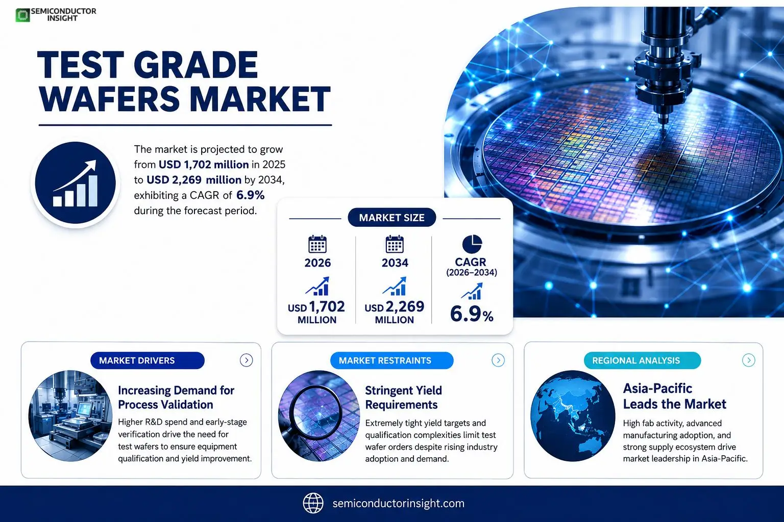
Test Grade Wafers market was valued at USD 1,702 million in 2025 and is expected to reach USD 2,269 million by 2034, reflecting a CAGR of 6.9 % over the forecast horizon.
In semiconductor fabrication a Test Wafer functions as a non‑product substrate used to qualify equipment, fine‑tune process recipes and support metrology or calibration activities. These wafers replicate production‑grade silicongenerally single‑crystal CZ or FZwith controlled orientation, resistivity windows and surface finishes such as polished or epitaxial layers. Because they never ship as final devices they safeguard yield during ramp‑up while enabling systematic design‑of‑experiments without consuming valuable product capacity.The upward trend stems from several forces: heightened metrology intensity in advanced nodes compels more frequent tool qualification; sustainability pressures accelerate extensive reuse through precision reclaim cycles; and the industry’s shift toward 200 mm/300 mm diameters tightens geometry tolerances, boosting demand for high‑stability test wafers. Leading suppliersincluding Shin‑Etsu Chemical, SUMCO, Wafers and Siltronic AGhave broadened reclaimed‑wafer services and introduced patterned calibration variants to meet these evolving requirements.
MARKET DRIVERS
Increasing Demand for Early‑Stage Process Validation
Foundry customers are allocating a larger share of their R&D budgets to pre‑production verification, because defects discovered after tape‑out become dramatically more expensive to remediate. Test Grade Wafers Market benefits from this shift, as manufacturers seek wafer‑level test structures that emulate final‑product behavior without the cost of full‑scale production runs.
Shift Toward Heterogeneous Integration
Mix‑and‑match of silicon, compound semiconductors, and advanced packaging introduces new failure modes that cannot be captured by legacy test suites. Test grade wafers engineered for heterogeneous stacks provide a timely answer, allowing designers to isolate electrical and thermal interactions early in the design cycle. Companies that embed these test assets into their development flow report shorter time‑to‑market and lower engineering change orders.
➤ “Early wafer‑level testing now accounts for a decisive portion of yield improvement strategies across leading fabs.”
Regulatory scrutiny of defect densities in safety‑critical applications, such as autonomous driving and medical devices, further amplifies the need for reliable test grade wafers. Suppliers that can certify compliance while delivering rapid turnaround are positioning themselves as indispensable partners in the value chain.
MARKET CHALLENGES
Complexity of Test Grade Wafer Qualification
Qualification protocols for test grade wafers differ from those applied to production wafers, yet many customers still rely on legacy qualification data. This mismatch creates uncertainty about the predictive power of test structures, prompting some designers to revert to more conservative, higher‑cost approaches.
Other Challenges
Cost Sensitivity
While test grade wafers are cheaper than full‑scale production wafers, the incremental cost can still be significant for low‑volume programs. Budget‑constrained startups often postpone test‑grade purchases, opting instead for limited in‑house prototypes, which may delay defect detection.
MARKET RESTRAINTS
Stringent Yield Requirements
As fabs push wafer yields beyond 90 percent, the margin for error in test grade wafers narrows. Even minor variations in test structure design can translate into misleading yield forecasts, causing some manufacturers to limit the volume of test grade wafers they order. This caution restricts market expansion despite broader industry interest.
MARKET OPPORTUNITIES
Emergence of AI‑Driven Test Platforms
Machine‑learning algorithms are being integrated into wafer‑test equipment to predict failure mechanisms from limited test data. When paired with specially designed test grade wafers, these platforms can accelerate root‑cause analysis and reduce the number of physical test cycles required.
Growth of Advanced Packaging Ecosystems
2.5 D/3 D stacking solutions demand bespoke test structures that expose inter‑die connectivity and thermal bottlenecks. Suppliers that develop test grade wafers tailored to these packaging formats stand to capture a sizable share of the evolving Test Grade Wafers Market.
Strategic Partnerships with Foundries
Joint development agreements between test grade wafer vendors and leading foundries enable co‑optimized design rules and faster qualification cycles. Such collaborations mitigate the qualification complexity described earlier and create a predictable pipeline for future product introductions.
Test Grade Wafers Market Trends
Rising Metrology Intensity Fuels Test Wafer Demand
Test Grade Wafers Market is feeling the impact of tighter process windows that modern fab lines require. As device geometries shrink, manufacturers rely on non‑product wafers to qualify new equipment, tune complex recipes, and verify design‑of‑experiments outcomes. Because a single test wafer can reproduce a full production stack, it serves as a low‑risk platform for yield protection. The need for high‑precision thickness, etch‑rate, and particle‑count data has doubled the frequency of test‑run cycles in the past five years, translating into a steady uplift in wafer orders. This operational shift explains why the market, valued at roughly $1,702 million in 2025, is charting a clear upward path while remaining insulated from end‑product volatility.
Other Trends
Cost‑Efficiency Through Reclaim and Reuse
Reclaim operations have become a core lever for cost containment in Test Grade Wafers Market. By stripping residual films, polishing the silicon substrate, and performing metal‑impurity removal, vendors extend wafer life across multiple test cycles. Advanced reclaim cycles now achieve cleanliness comparable to virgin wafers, allowing fabs to replace a fresh wafer only after several hundred uses. This approach not only trims material spend but also aligns with sustainability targets that many semiconductor clusters have adopted. The economics are evident: a reclaimed wafer can reduce per‑unit cost by 30 % while preserving the tight TTV and bow specifications that metrology teams demand.
Larger Diameter Adoption Reshapes Supply Chain
Another observable movement within Test Grade Wafers Market is the migration toward 200 mm and 300 mm formats. As fabs retire legacy 150 mm lines, the demand for larger‑diameter test wafers surges, pushing suppliers to invest in upgraded crystal growth and polishing capabilities. This transition intensifies the importance of crystalline uniformityCZ and FZ ingots are now routinely specified to meet the tighter geometry tolerances required for 300 mm processing. The shift also pressures smaller‑diameter producers to consolidate or exit, consolidating market share among a handful of players equipped to deliver the requisite surface quality at scale. For customers, the move translates into fewer handling steps and improved correlation between test and production runs, reinforcing the strategic value of standardized large‑diameter test wafers.
COMPETITIVE LANDSCAPE
Key Industry Players
Competitive forces shaping the Test Grade Wafers market
Shin‑Etsu Chemical, SUMCO and Wafers dominate the supply of virgin test‑grade silicon wafers, together accounting for roughly half of worldwide shipments. Their extensive crystal‑pulling capacity, spanning both Czochralski (CZ) and Float‑Zone (FZ) architectures, enables rapid configuration of orientation, resistivity and surface finish to meet fab‑specific qualification cycles. The market is organized as a three‑tier ecosystem: Tier‑1 wafer makers provide the baseline virgin stock, Tier‑2 reclaim specialists such as RS Technologies extend wafer life through sophisticated stripping and polishing, while Tier‑3 providers deliver patterned calibration artifacts that mimic production‑line geometry. This structure creates a clear hierarchy where the leading manufacturers set the price floor and technical standards, while downstream players compete on value‑add services, turnaround time and cost‑efficiency of reclaimed wafers.Beyond the dominant trio, a cohort of niche innovators is reshaping segment dynamics. Siltronic AG’s aggressive transition to 300 mm test wafers tightens geometry tolerances and forces competitors to upgrade tooling. SK Siltron and FST Corporation leverage deep relationships with Asian foundries to supply region‑specific doping windows and thin‑film coated test wafers. Reclaim specialists like RS Technologies and Kinik differentiate through metal‑impurity removal processes that approach virgin‑quality cleanliness, reducing fab‑level capex on dummy inventory. Smaller Chinese playersincluding Zhonghuan Advanced Semiconductor Materials, Hangzhou Lion Microelectronics and Shanghai Advanced Silicon Technologyfocus on cost‑effective reclaimed blanks and localized support, capitalising on the sustainability pressure driving fabs toward higher wafer reuse rates. The combined effect is a market where scale, technical versatility and reclaim expertise dictate competitive positioning.
List of Key Test Grade Wafers Companies Profiled
- Shin‑Etsu Chemical
- Shin‑Etsu Chemical
- SUMCO
- SUMCO
- Wafers
- Siltronic AG
- Siltronic AG
- SK Siltron
- FST Corporation
- Wafer Works Corporation
- National Silicon Industry Group (NSIG)
- Zhonghuan Advanced Semiconductor Materials
- Hangzhou Lion Microelectronics
- RS Technologies
- RS Technologies
- Kinik
- Phoenix Silicon International
- Hamada Rectech
Segment Analysis:
| Segment Category | Sub-Segments | Key Insights |
| By Type |
|
Virgin Test Wafer remains the preferred choice for initial tool qualification because it delivers the most consistent baseline geometry and surface quality. – Provides unmatched mechanical stability for high‑precision metrology. – Enables rapid recipe development without contaminant carry‑over concerns. – Serves as a reference point for subsequent reclaimed cycles, anchoring process control across fab phases. |
| By Application |
|
Tool Qualification dominates the application landscape as fabs rely on test wafers to de‑risk new equipment. – Allows engineers to capture baseline etch rates and film thickness before production runs. – Supports repeatable recipe tuning, shortening ramp‑up time for new process nodes. – Facilitates cross‑tool comparability, ensuring consistent output across multiple chambers. |
| By End User |
|
Foundries exhibit the strongest demand for test wafers because of the high volume of equipment cycles and the need for stringent process stability. – Leverage reclaimed wafers to control cost while maintaining calibrated performance. – Require a diverse portfolio of orientation and doping options to mirror customer product specifications. – Emphasize rapid turnaround from wafer suppliers to keep fab line uptime high. |
| By Wafer Configuration |
|
Crystal Orientation is a decisive factor for replicating production‑grade behavior on test wafers. – <100> wafers provide a baseline for most logic processes, simplifying comparison. – <111> variants are favored for power devices where anisotropic etch characteristics matter. – Precise orientation control reduces variability in thickness measurements, enhancing the reliability of metrology data. |
| By Supply Chain Role |
|
Reclaim & Value‑Add Providers are gaining strategic importance as sustainability and cost efficiency become central to fab operations. – Offer multi‑cycle reclamation that approaches virgin‑grade surface cleanliness. – Provide optional thin‑film deposition (e.g., oxide, nitride) to create ready‑to‑use calibration targets. – Enable closed‑loop supply models where reclaimed wafers are cycled back to the fab within short lead times, reducing inventory pressure. |
Regional Analysis: Test Grade Wafers Market
Asia-Pacific
Leading players have expanded clean‑room footprints to accommodate rising specimen throughput, yet they resist over‑building by adopting modular equipment that can be re‑configured as test specifications evolve. This tactical flexibility sustains profitability while meeting fluctuating demand cycles.
Recent disruptions have prompted firms to diversify sources of high‑purity chemicals and to secure secondary logistics hubs. Such measures mitigate single‑point failures, ensuring uninterrupted wafer flow to downstream assembly lines.
Government incentives targeting silicon‑based innovation have lowered capital outlays for test‑grade production lines. Coupled with relaxed export controls, these policies encourage inbound investment and bolster the region’s competitive edge.
Tier‑1 device manufacturers prioritize suppliers that can deliver sub‑micron uniformity, whereas emerging fabless players value cost‑effective options with rapid turnaround. Vendors tailoring service packages to these distinct needs gain a strategic advantage.
North America
North America retains a robust foothold in Test Grade Wafers Market, anchored by a concentration of R&D laboratories that stress reliability testing for high‑performance computing chips. The region’s emphasis on silicon‑photonic integration has spurred demand for wafers with exceptionally low defect densities, prompting local suppliers to invest in inline metrology upgrades. While labor costs are higher than in Asia‑Pacific, the premium placed on intellectual property protection and rapid prototype cycles justifies the expense for many innovators. Companies that can synchronize design verification with supply timelines secure recurring contracts from leading OEMs, reinforcing the continent’s strategic relevance.
Europe
European stakeholders approach Test Grade Wafers Market with a focus on sustainability and precision engineering. Initiatives under the EU’s Green Chip agenda encourage the adoption of environmentally‑friendly processing chemicals, nudging manufacturers toward cleaner‑room practices. Moreover, the continent’s strong automotive semiconductor segment demands test wafers that can endure extreme thermal cycles, driving niche product development. Collaborative consortia between universities and fab operators foster talent pipelines, ensuring that expertise in advanced verification techniques remains abundant. For suppliers, aligning with these sustainability standards opens doors to premium contracts in sectors where compliance is non‑negotiable.
South America
South America is gradually emerging as a supplemental hub for Test Grade Wafers Market, benefitting from lower operational overhead and growing governmental support for technology parks. Local fabs are increasingly targeting mid‑range devices, where cost‑sensitive test wafers are essential. Although the region lacks the deep‑node expertise of its northern counterparts, it compensates with a flexible labor market and the ability to offer rapid scale‑up for niche applications. Partnerships with multinational vendors are beginning to materialize, providing technology transfer that elevates local capabilities and expands the market’s geographic breadth.
Middle East & Africa
The Middle East & Africa corridor offers a mixed outlook for Test Grade Wafers Market. In the United Arab Emirates, sovereign wealth funds have financed state‑of‑the‑art semiconductor labs, positioning the emirate as a testing gateway for Gulf‑based electronics firms. Conversely, many African economies are still at an early stage of semiconductor adoption, yet they exhibit strong appetite for affordable test solutions as mobile and IoT penetration rises. Companies that can tailor pricing models and provide remote verification services are likely to capture early market share, laying groundwork for future expansion as regional infrastructure matures.
Report Scope
This market research report provides a comprehensive analysis of the Test Grade Wafers Market , covering the forecast period 2026–2034. It offers detailed insights into market dynamics, technological advancements, competitive landscape, and key trends shaping the industry.
Key focus areas of the report include:
- Market Overview: The report begins with an overview outlining its current market scenario, key growth indicators, and industry transformation drivers. It discusses macroeconomic factors, demand–supply balance, regulatory landscape, and the strategic role of semiconductors in powering advancements across industries such as automotive, telecommunications, consumer electronics, and industrial automation.
- Market Size & Forecast: Historical data and future projections for revenue, unit shipments, and market value across major regions and segments.
- Segmentation Analysis: Detailed breakdown by product type, technology, application, and end-user industry to identify high-growth segments and investment opportunities.
- Regional Insights: Insights into market performance across North America, Europe, Asia-Pacific, Latin America, and the Middle East & Africa, including country-level analysis where relevant.
- Competitive Landscape: Profiles of leading market participants, including their product offerings, R&D focus, manufacturing capacity, pricing strategies, and recent developments such as mergers, acquisitions, and partnerships.
- Technology Trends & Innovation: Assessment of emerging technologies, integration of AI/IoT, semiconductor design trends, fabrication techniques, and evolving industry standards.
- Market Drivers & Restraints: Evaluation of factors driving market growth along with challenges, supply chain constraints, regulatory issues, and market-entry barriers.
- Stakeholder Insights: Insights for component suppliers, OEMs, system integrators, investors, and policymakers regarding the evolving ecosystem and strategic opportunities.
Primary and secondary research methods are employed, including interviews with industry experts, data from verified sources, and real-time market intelligence to ensure the accuracy and reliability of the insights presented.
FREQUENTLY ASKED QUESTIONS:
What is the current market size of Test Grade Wafers Market?
-> Test Grade Wafers Market was valued at USD 1702 million in 2025 and is expected to reach USD 2269 million by 2034, at a CAGR of 6.9% during the forecast period.
Which key companies operate in Test Grade Wafers Market?
-> Key players include Shin-Etsu Chemical, SUMCO, Wafers, Siltronic AG, SK Siltron, FST Corporation, Wafer Works Corporation, National Silicon Industry Group (NSIG), Zhonghuan Advanced Semiconductor Materials, Hangzhou Lion Microelectronics, among others.
What are the key growth drivers?
-> Key growth drivers include increasing metrology intensity, tighter process windows in advanced manufacturing, cost‑sustainability pressures driving wafer reclaim, and the shift toward larger 200/300 mm wafer diameters.
Which region dominates the market?
-> Asia dominates the market, driven by high fab activity and adoption of larger wafer formats, while North America and Europe also hold significant shares.
What are the emerging trends?
-> Emerging trends include advancements in wafer reclaim processes, increased use of 200/300 mm test wafers, and development of patterned/calibration wafers for precise metrology.
Get Sample Report PDF for Exclusive Insights
Report Sample Includes
- Table of Contents
- List of Tables & Figures
- Charts, Research Methodology, and more...
 Download Sample Report PDF




