
Top 10 Leading Companies in Laser Annealing Equipment Market in 2026
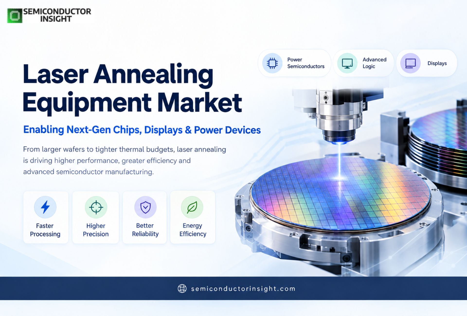
Laser annealing has moved from a specialized tool to a core enabler across power semiconductors, advanced logic nodes, and high-resolution displays. The technology delivers localized, ultra-fast heating that activates dopants, forms silicides, repairs crystal damage, and crystallizes thin films while protecting sensitive underlying structures.
Demand surged in 2025-2026 as SiC power devices scaled to larger wafers, 400-layer NAND processes tightened thermal budgets, and display makers shifted to bigger glass generations. The following companies stand out through proven system deployments, specialized laser architectures, and recent production milestones that directly advance these applications.
JSW Aktina’s Excimer Platforms Driving Large-Substrate Crystallization
JSW Aktina has installed more than 240 excimer laser annealing systems since 1995 across display fabs in China, Japan, South Korea, Taiwan, and Singapore. Its systems convert amorphous silicon on glass into low-temperature polycrystalline silicon for high-resolution TFTs. In 2025 the company delivered the world’s first float-type system supporting 8.6-generation substrates measuring 2,290 mm by 2,620 mm, following an earlier order for eight such units from Chinese customers.
These platforms handle Gen 4.5 (730 × 920 mm) through Gen 10.5 (2,940 × 3,370 mm) glass and incorporate multi-cycle handling that lifts productivity roughly 20 percent while cutting cost of ownership. Twin-Vyper and Tri-Vyper laser configurations paired with specialized optical systems such as LB1300-G8 deliver the beam uniformity needed for OLED tablet, foldable, and large-monitor panels. Parallel work on silicidation tools for SiC wafers further extends the same high-power gas-laser control technology into power-device manufacturing lines that began receiving units in 2025.
Sumitomo Heavy Industries’ Hybrid and UV Systems Expanding Power-Device Activation
Sumitomo Heavy Industries has shipped more than 150 laser annealing systems worldwide since its first delivery in 2004, establishing a strong position in backside activation for IGBTs and ohmic-contact formation on SiC. Its SWA Green/Hybrid series combines solid-state and long-wavelength lasers to enable double-pulse processes that activate dopants to depths of 7 µm while holding in-plane uniformity at σ ≤ 1 percent. Models support both 200 mm and 300 mm wafers and handle wafers as thin as 70 µm.
The SWA UV series uses a high-speed OPTSWING scanning method and top-hat beams for SiC ohmic contacts on substrates up to 8 inches. In late 2024 the company integrated its laser operations with its ion-implanter subsidiary and acquired the LASSE laser-annealing business, creating a combined offering that links implant and anneal steps. Demo systems remain available for process evaluation, helping device makers qualify the tools for next-generation power semiconductors.
SCREEN’s Nanosecond Platforms Enabling Low-Thermal-Budget Surface Engineering
Through its LASSE affiliate, SCREEN offers nanosecond UV laser annealers such as the LT-3100 and QA-3000 that heat only the wafer surface in sub-microsecond timescales. These systems perform melt annealing for dopant activation, thin-film crystallization, defect repair, and surface smoothing on wafers ranging from small power-device sizes to full 300 mm. Temperature cycles complete in under 200 ns, protecting fragile 3D structures and ultra-thin wafers below 40 µm.
Step-and-repeat exposure covers individual dies or full fields without stitching, and real-time monitoring supports both mass-production stability and rapid process development on a single wafer. The tools address backside metallization on SiC and deep junction activation in Si IGBTs, giving manufacturers a flexible platform that meets the thermal-budget constraints of advanced nodes.
Veeco’s Spike and Nanosecond Tools Advancing Leading-Edge Logic and Memory
Veeco’s laser-spike annealing systems, including the LSA 101 and LSA 201, deliver millisecond-scale high-temperature processing that activates dopants without diffusion in advanced logic and memory. Dual-beam technology maintains activation while eliminating deactivation, and closed-loop temperature control ensures within-die and die-to-die uniformity.
In late 2024 the company shipped its first NSA500 nanosecond annealing system to a leading-edge customer for high-volume production of 2 nm gate-all-around chips; evaluation programs continue at additional logic and memory makers. The nanosecond platform targets shallow surface layers for backside power delivery, contact annealing, void removal, and grain growth. A separate 2025 evaluation shipment of an LSA system into a major DRAM R&D line further expanded the technology’s reach into high-bandwidth memory stacks.
Applied Materials’ Thermal Solutions Supporting Advanced Node Integration
Applied Materials supplies laser-annealing platforms that form part of its broader thermal-process portfolio used in leading-edge logic and memory flows. The systems enable precise activation and material modification at nodes where conventional furnace anneals exceed thermal budgets.
Recent customer deployments support channel-length control and threshold-voltage tuning on 3 nm-class production lines, while ongoing platform refinements address the uniformity and throughput demands of 300 mm wafers. These tools sit alongside other materials-engineering steps that together account for a substantial portion of wafer-fab equipment spending at advanced nodes.
To find out more, feel free to browse our latest updated report: https://semiconductorinsight.com/report/laser-annealing-equipment-market/
Hitachi’s Precision Laser Approaches for Specialized Semiconductor Flows
Hitachi contributes laser-based thermal solutions within its semiconductor-equipment offerings, focusing on applications that require tight spatial and temporal control. The systems support dopant activation and interface engineering in power devices and advanced packaging structures.
Integration with Hitachi’s broader process know-how allows customers to combine annealing with upstream implant or downstream metallization steps, improving overall process windows for devices that cannot tolerate bulk heating.
YAC BEAM’s Dual-Wavelength Tools Targeting Backside Power-Device Processing
YAC BEAM designs laser annealers specifically for Si-IGBT backside activation and SiC electrode ohmicization. Dual-wavelength systems (typically green and infrared) control anneal depth between 1 µm and 10 µm while keeping the non-irradiated surface below 100 °C even on wafers thinner than 100 µm.
Continuous-wave lasers combined with rotating stages deliver high throughput approximately five 6-inch wafers per hour for SiC ohmic processes. Contact resistance reaches the 10⁻⁴ to 10⁻⁶ Ω·cm² range, and the tools accommodate various metal stacks under Class 1000 or nitrogen atmospheres. These features make the platforms practical for high-volume power-semiconductor lines that rely on thin wafers.
EO Technics’ Flexible Wavelength Platforms for Crystallization and Silicide Formation
EO Technics offers laser annealers covering both front-end wafer processes and power-device applications. Systems such as the LAton series perform crystallization, dopant activation, surface melting, and void-seam removal on silicon wafers, with wavelength and beam-shape options tailored to each process.
Higher-end models improve energy and pulse-shape stability while raising productivity by about 25 percent over base configurations. Dedicated power-device tools form nickel silicide for SiC ohmic contacts and activate IGBT backside dopants, again with selectable wavelengths and real-time process monitoring. The modular optical design allows rapid adaptation to new device stacks.
Beijing U-Precision’s Modular SiC Annealers Supporting Thin and Warped Wafers
Beijing U-Precision develops SiC-specific laser annealing equipment with modular architecture suitable for both research and production. The systems handle 4-inch and 6-inch ultra-thin or highly warped wafers with precise positioning and controlled oxygen levels below 10 ppm inside the process chamber.
Visual alignment, real-time parameter monitoring, and flexible integration options enable efficient transfer between development and high-volume lines. These capabilities address the mechanical challenges unique to SiC substrates while delivering the localized heating required for dopant activation and contact formation.
Shanghai Micro Electronics Equipment’s Domestic Solutions for IGBT and SiC Flows
Shanghai Micro Electronics Equipment supplies laser annealing tools aimed at field-stop IGBT backside processing and SiC substrate treatment. The systems provide localized spike annealing that activates dopants without the bulk thermal load of conventional rapid thermal processing.
Patented beam-shaping and scanning approaches produce rectangular spots with controlled energy profiles, supporting uniform results across wafer surfaces. These platforms form part of China’s broader effort to localize power-semiconductor equipment and are already used in development and early production of advanced IGBT and SiC devices.

Comments (0)