
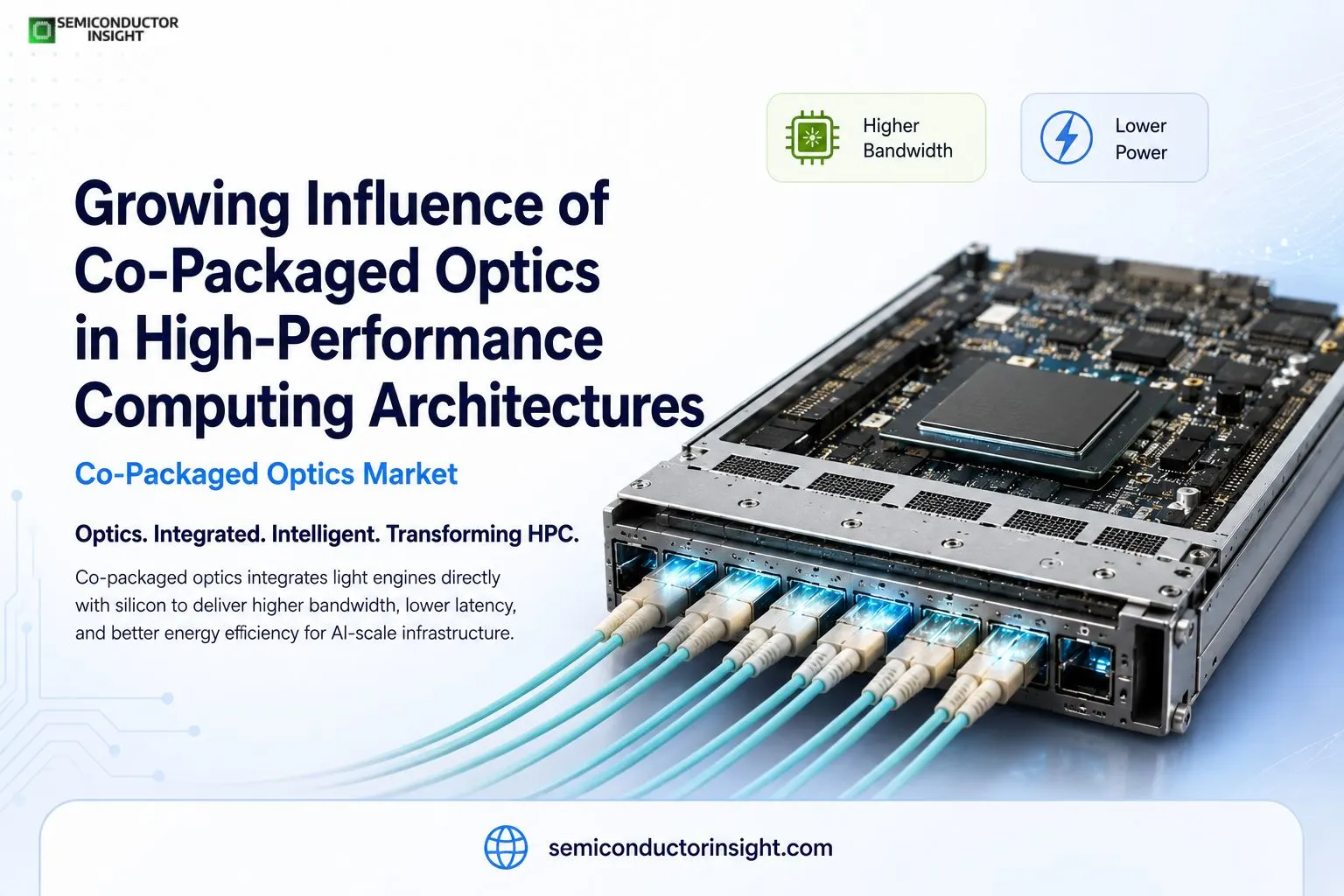
The Growing Influence of Co-Packaged Optics Market in High-Performance Computing Architectures
The semiconductor industry is entering a phase where data movement has become just as important as processing power itself. As artificial intelligence models grow larger and cloud computing workloads become more complex, conventional electrical interconnects are struggling to keep pace with bandwidth and energy requirements. This shift is bringing co-packaged optics market into the spotlight as one of the most closely watched areas in advanced semiconductor infrastructure.
Co-packaged optics, commonly referred to as CPO, integrates optical communication components directly alongside switching silicon within the same package. Instead of relying solely on traditional pluggable optical modules positioned farther from the processor, CPO shortens communication paths and significantly improves data transmission efficiency. The technology is rapidly gaining attention among hyperscale cloud providers, networking companies, and semiconductor manufacturers looking to solve growing data centre bottlenecks.
A Closer Look at Our Latest Related Study and Key Findings: https://semiconductorinsight.com/report/hot-pluggable-optical-modules-market/
AI Data Centres Are Pushing Existing Architectures to Their Limits
- The global expansion of generative AI has dramatically increased networking pressure inside modern data centres. Training large language models requires thousands of GPUs and accelerators to exchange enormous volumes of information simultaneously.
- According to technical disclosures from leading cloud infrastructure companies, AI clusters can consume several megawatts of power while transferring data across interconnected systems at unprecedented speeds. Conventional copper interconnects face thermal limitations, signal degradation, and rising power consumption as bandwidth scales higher.
- This is where co-packaged optics is becoming increasingly important. By integrating optics closer to switching ASICs, data transmission can occur with lower latency and reduced energy loss. Some advanced networking systems are already targeting 51.2 terabit-per-second switch capacities, creating demand for more efficient optical communication architectures.
Silicon Photonics Is Moving Into Mainstream Semiconductor Strategy
One of the strongest forces supporting co-packaged optics market is the rapid progress in silicon photonics. Semiconductor manufacturers are increasingly combining photonic circuits with electronic components to improve speed and power efficiency.
Major industry players including Broadcom Inc., and Cisco Systems have publicly discussed investments in optical interconnect technologies for next-generation switching platforms.
In recent demonstrations, several semiconductor companies showcased 800G and 1.6T optical networking solutions designed for hyperscale AI environments. These platforms are expected to support the rising computational intensity associated with machine learning inference and distributed AI training systems.
Industry organizations such as the Consortium for On-Board Optics are also encouraging standardization efforts that could accelerate commercial deployment across networking ecosystems.
Energy Consumption Is Becoming a Boardroom-Level Concern
Modern data centres are facing mounting electricity demands. According to reports from the International Energy Agency, global data centre electricity consumption could continue rising significantly due to AI-related workloads and expanding cloud infrastructure.
Networking equipment contributes heavily to thermal output inside server environments. Traditional electrical interconnects require higher power as transmission distances and bandwidth demands increase. Co-packaged optics offers a practical way to reduce energy per transmitted bit while supporting denser networking architectures.
Some prototype systems have demonstrated energy efficiencies below 5 picojoules per bit in optical communication pathways, a figure closely monitored by semiconductor engineers working on sustainable AI infrastructure. Lower thermal stress also improves rack density potential inside hyperscale facilities.
Hyperscale Companies Are Quietly Accelerating Adoption
- Several hyperscale cloud operators are already evaluating co-packaged optical systems for future deployment strategies.
- While many projects remain confidential, ongoing collaborations between switch manufacturers, optical component developers, and cloud infrastructure firms have intensified over the past two years.
- AI-focused infrastructure expansion is a major reason behind this acceleration. Companies deploying large GPU clusters require networking systems capable of handling massive east-west traffic across distributed computing nodes.
- Optical connectivity is increasingly viewed as necessary rather than optional for maintaining scalable AI performance.
- Recent announcements surrounding advanced Ethernet switching platforms and optical I/O architectures indicate that the industry is steadily moving toward broader commercial integration.
- Research groups are also exploring photonic chiplets and optical fabrics that could redefine server-level communication over the next decade.
Why Semiconductor Packaging Is Becoming a Strategic Innovation Layer?
Co-packaged optics market is not solely about networking speed. It also reflects a broader transformation in semiconductor packaging philosophy. As Moore’s Law scaling becomes more challenging, companies are turning toward advanced integration methods to achieve performance gains.
- Packaging technologies now influence power efficiency, thermal management, signal integrity, and overall system scalability. Co-packaged optics represents a convergence of semiconductor engineering, photonics, advanced substrates, and high-density packaging techniques.
- For semiconductor manufacturers, the technology is becoming part of a larger strategy focused on heterogeneous integration. Instead of improving chips alone, companies are redesigning the entire communication architecture surrounding processors and accelerators.
As AI infrastructure investments continue expanding globally, co-packaged optics is steadily evolving from an experimental networking concept into a foundational component of next-generation semiconductor ecosystems.

Comments (0)