
Technology Evolution and Growth Dynamics in Semiconductor Equipment for BEOL Market
Semiconductor Equipment for BEOL Market is evolving rapidly as advanced packaging, AI chip demand, and high-density interconnect technologies reshape modern semiconductor manufacturing.
Now let’s go through the Growing Impact of BEOL Technologies in Modern Chip Manufacturing
The Back End of Line (BEOL) stage plays a crucial role in semiconductor fabrication as it focuses on forming metal interconnections that link millions or even billions of transistors on a chip. While the front-end process creates the transistors, BEOL enables electrical connectivity, allowing chips to perform complex computing tasks.
Modern chips can contain more than 100 billion transistors, making interconnect density and reliability a critical challenge for manufacturers. Semiconductor equipment used in BEOL processes includes deposition systems, etching tools, cleaning equipment, and chemical mechanical planarization tools designed specifically for metal layer formation.
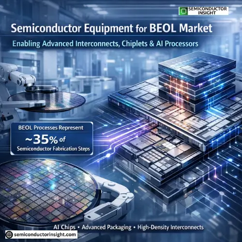
In advanced chip production, BEOL layers can exceed 15 metal layers in high-performance processors. This complexity has increased demand for precise manufacturing tools capable of maintaining nanoscale alignment and defect control. Approximately 35% of semiconductor fabrication steps are now associated with BEOL processes, highlighting their growing importance in overall chip production.
Growing Complexity of Interconnect Architecture
As semiconductor nodes continue shrinking below 5 nm, interconnect architecture has become one of the most technically demanding aspects of chip manufacturing. Smaller geometries increase resistance and signal delay in metal lines, requiring advanced materials and process technologies.
Copper interconnects remain dominant, accounting for nearly 80% of BEOL metallization in modern logic devices. However, emerging materials such as cobalt and ruthenium are gaining attention due to their improved reliability at smaller dimensions.
Additionally, advanced dielectric materials are increasingly used to reduce parasitic capacitance. Low-k dielectric materials are utilized in more than 60% of high-performance semiconductor designs, improving signal transmission speed while reducing power consumption.
These evolving design requirements are pushing semiconductor manufacturers to adopt highly specialized equipment capable of delivering atomic-level precision during deposition, patterning, and polishing steps.
Feel Free to Reach Our Most Recent Updates of the Report:
https://semiconductorinsight.com/report/semiconductor-equipment-for-beol-market/
Advanced Packaging and Chiplet Integration
- The rise of Advanced Packaging technologies has significantly increased the importance of BEOL equipment. Chiplet architectures, heterogeneous integration, and 3D stacking techniques rely heavily on BEOL processes to create high-density interconnects between multiple dies.
- Nearly 45% of newly developed high-performance computing processors now use some form of chiplet-based architecture. This approach allows manufacturers to combine multiple specialized chips into a single package, improving performance and production flexibility.
- Technologies such as through-silicon vias (TSVs) and hybrid bonding are becoming increasingly common in advanced packaging. In some leading-edge chips, interconnect pitch can be reduced to less than 10 micrometers, enabling faster communication between chip components.
- As these technologies become mainstream, equipment demand for wafer bonding, dielectric deposition, and precision etching tools is rising significantly across semiconductor fabrication facilities.
AI and Data Center Chips Driving Equipment Demand
The global surge in artificial intelligence applications has created unprecedented demand for high-performance semiconductors. AI accelerators and data center processors require extremely dense interconnect networks to support massive data processing workloads.
Modern AI chips often incorporate thousands of processing cores and require multiple metal layers to ensure efficient signal routing. In advanced AI processors, interconnect layers can represent more than 50% of the chip’s total fabrication complexity.
Semiconductor manufacturers are therefore investing heavily in BEOL equipment capable of supporting ultra-fine patterning and defect-free metallization processes. Equipment designed for extreme precision and high throughput is becoming essential as production volumes increase.
The data center industry itself accounts for nearly 30% of global demand for high-performance logic chips, which directly contributes to rising investments in BEOL manufacturing capabilities.
Regional Manufacturing Expansion
Semiconductor manufacturing expansion across several regions is strengthening the demand for BEOL equipment. Governments worldwide are supporting domestic semiconductor production through industrial policy initiatives and technology investment programs.
East Asia currently represents more than 60% of global semiconductor fabrication capacity, driven by large-scale manufacturing facilities in Taiwan, South Korea, and Japan. However, new fabrication plants are emerging across North America and Europe as part of supply chain diversification efforts.
More than 70 new semiconductor fabrication facilities have been announced globally in recent years. Each facility requires hundreds of specialized tools dedicated to BEOL processing stages, including deposition, etching, cleaning, and inspection equipment.
This geographic expansion is expected to reshape equipment supply chains and accelerate innovation in manufacturing technologies.
Automation and Smart Manufacturing in BEOL Facilities
- Modern semiconductor fabs are increasingly adopting Automation and data-driven manufacturing systems to improve production efficiency and yield. BEOL processes involve extremely delicate steps where even microscopic contamination can lead to device failure.
- Smart manufacturing platforms integrate sensors, AI-driven process monitoring, and predictive maintenance technologies. These systems help detect equipment anomalies early and optimize process parameters in real time.
- More than 75% of newly built semiconductor fabs now incorporate advanced automation systems designed to support high-volume manufacturing environments. Automated wafer handling and robotic systems also reduce the risk of contamination and improve operational efficiency.
- As semiconductor devices become more complex, automation technologies will play a central role in maintaining high production yields.
Lastly, the long-term outlook for Semiconductor Equipment for BEOL Market remains strong as global demand for advanced chips continues to expand. Technologies such as artificial intelligence, autonomous systems, and next-generation telecommunications are pushing semiconductor performance requirements to new levels.
Manufacturers are increasingly exploring alternative interconnect materials, novel lithography methods, and hybrid bonding techniques to overcome scaling limitations. These innovations are expected to reshape BEOL manufacturing processes over the coming decade.
Additionally, the transition toward 3D Integration and chiplet architectures will further increase the complexity of back-end manufacturing stages. As a result, semiconductor equipment suppliers will continue developing highly specialized tools designed to support next-generation chip fabrication.
With semiconductor devices becoming central to nearly every digital technology, BEOL equipment will remain a critical component in enabling faster, more efficient, and highly integrated computing systems across industries.

Comments (0)