
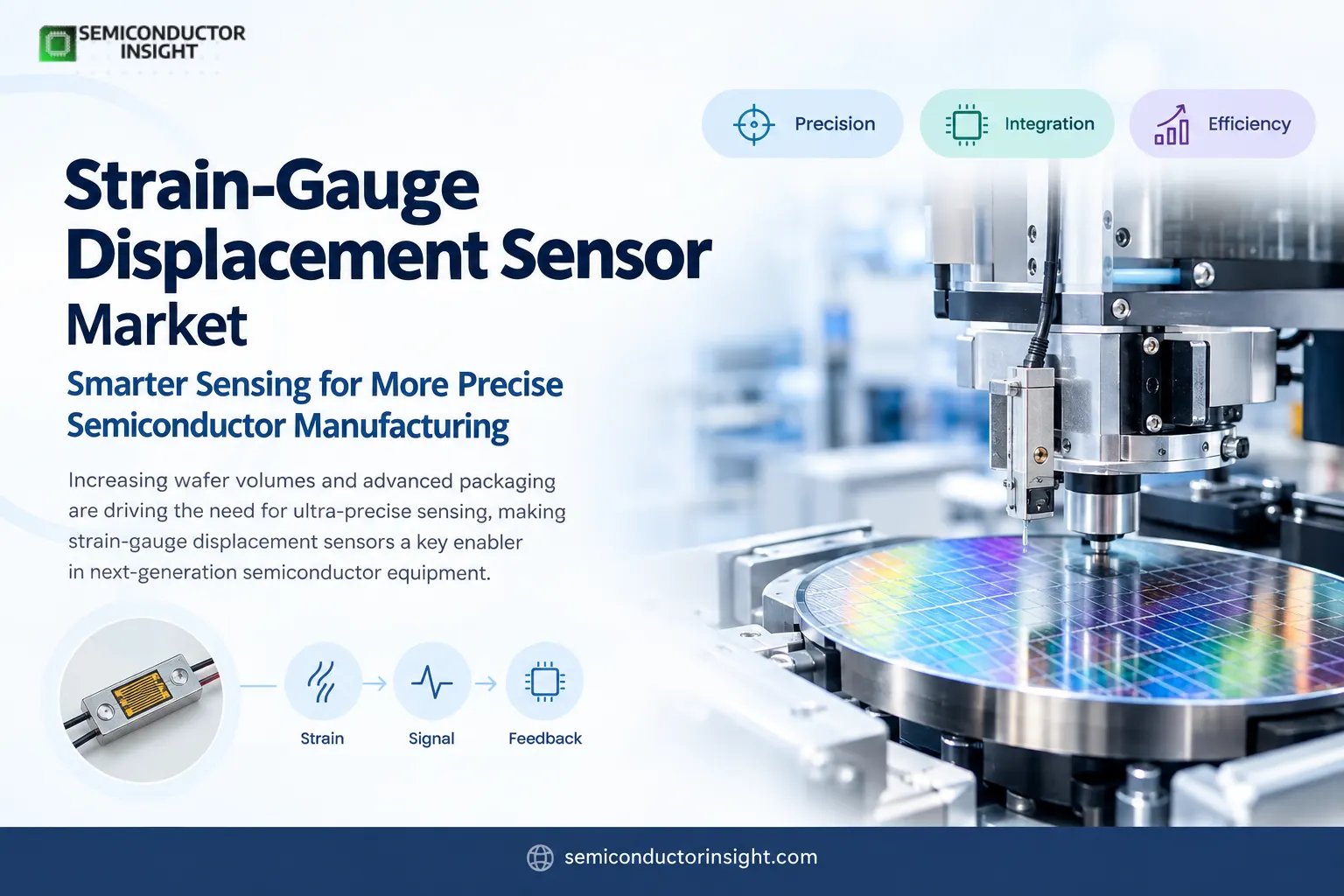
Strain Gauge vs. Capacitive Displacement Sensors Market 2026: Precision Technology Comparison
A semiconductor fabrication line can contain equipment where mechanical movement is measured in fractions of a millimeter while the resulting process can determine the quality of structures manufactured across an entire wafer. This is where strain-gauge displacement sensing becomes relevant. Instead of relying only on optical measurement, a strain-gauge displacement sensor converts mechanical deformation into an electrical signal, allowing movement, position, force or deflection to be monitored through an integrated sensing structure.
The technology is becoming particularly interesting as semiconductor equipment moves toward tighter process control, advanced packaging and increasingly complex wafer-processing architectures.
The Measurement Principle behind the Sensor
- A strain gauge responds to mechanical deformation through a change in electrical resistance. When mounted on a flexure or mechanical element, even a very small displacement can produce measurable strain. A Wheatstone bridge can then convert the resistance change into an electrical output.
The basic measurement chain is:
Mechanical movement → Flexure deformation → Strain change → Resistance variation → Bridge signal → Digital measurement → Equipment feedback
- The approach is not new, but its value lies in how easily the sensing element can be integrated into compact mechanical assemblies.
- Semiconductor-grade strain gauges can also provide substantially higher sensitivity than conventional metal foil gauges, although temperature effects and long-term stability must be carefully managed.
Why Wafer Manufacturing Creates a Different Sensing Problem
Semiconductor equipment is operating against a background of increasingly demanding wafer specifications. SEMI reported worldwide silicon-wafer shipments of 3,573 million square inches in the second quarter of 2026, up 7.4% from 3,327 million square inches in the same quarter of 2025. The organization attributed the continued demand partly to AI-related applications extending beyond advanced logic and memory into power devices and photonics.
At the same time, 300 mm wafers remain central to high-volume semiconductor manufacturing. This makes equipment-level movement, positioning and force control increasingly important because a small mechanical inconsistency can influence processing uniformity across a large substrate.
Where Displacement Meets Semiconductor Equipment
The sensor is not necessarily measuring the wafer itself. In many cases, it monitors the mechanical element responsible for positioning, loading, pressing, alignment or process control.
Relevant equipment functions include wafer handling mechanisms, precision stages, bonding systems, polishing equipment, test fixtures, robotic assemblies and force-controlled tooling.
This creates a broader sensing architecture:
Sensor element → Mechanical structure → Amplification or bridge circuit → Signal conditioning → Controller → Equipment adjustment
The resulting information can be used to detect movement, verify positioning, identify abnormal loading or provide feedback to a machine-control system.
A New Role in Advanced Packaging
- Advanced packaging is changing the measurement environment.
- Processes such as thermocompression bonding, wafer-level processing and heterogeneous integration require increasingly controlled mechanical interactions between components.
- A 2026 technical article in Silicon Semiconductor highlighted the growing importance of precision sensing in semiconductor manufacturing processes including grinding, chemical-mechanical polishing and thermocompression The article also noted that traditional MEMS and strain-gauge approaches are being reassessed as equipment requirements become more demanding.
- This does not eliminate strain-gauge sensing. Instead, it places greater emphasis on selecting the right sensor architecture for each mechanical measurement point.
The Scale Can Be Surprisingly Small
A strain-gauge displacement sensor does not need a large measurement body. Commercial strain-gauge displacement technology already demonstrates compact measurement ranges. HBM’s DD1, for example, provides displacement measurement of ±2.5 mm and an accuracy class of 0.1.
Academic work has also demonstrated strain-gauge displacement transducers designed around a 0–10 mm measurement range, illustrating how the technology can be configured around relatively short mechanical travel.
The important point is that semiconductor equipment does not always require a sensor capable of measuring centimeters of travel. Many applications instead need repeatable measurement within a tightly defined mechanical window.
Silicon Itself Is Becoming Part of the Sensing Story
Semiconductor strain gauges use the piezoresistive characteristics of doped silicon. When mechanical stress changes the structure of the sensing element, its electrical resistivity changes. This provides high sensitivity while enabling extremely compact sensing structures.
TE Connectivity describes silicon semiconductor strain gauges as devices based on doped silicon elements whose resistivity changes with mechanical strain. The technology can be fabricated directly on silicon or attached to a carrier, depending on the design.
That connection between semiconductor processing and sensing technology gives the segment an unusual position within the broader sensor ecosystem.
From Sensor Output to Machine Intelligence
Modern semiconductor equipment increasingly treats sensor data as a control input rather than a simple measurement.
A simplified closed-loop sequence looks like this:
Measure → Compare → Correct → Re-measure → Confirm
For example, if a mechanical stage does not reach its intended position, the sensor signal can be compared with the expected position and used by the control system to identify deviation. In production equipment, this type of feedback can support repeatability, preventive maintenance and process verification.
Macnica’s STREAL platform illustrates the direction toward embedded semiconductor-grade strain sensing, offering compact modules designed to capture force, load and torque information with resolution down to 0.1 microstrain in suitable applications.
The Industry Numbers Show Why Precision Matters
The semiconductor manufacturing environment is operating at enormous physical scale. SEMI reported 12,973 million square inches of silicon-wafer shipments during 2025, representing a 5.8% increase from 2024. The organization specifically identified strong demand for 300 mm wafers associated with advanced logic and high-bandwidth memory.
The quarterly trajectory continued in 2026. Shipments reached 3,275 million square inches in Q1 and 3,573 million square inches in Q2.
These figures demonstrate the volume of manufacturing activity in which precision equipment operates, even though the strain gauge itself may occupy only a very small physical area.
You Can Freely Surf Our Latest Updated Report Here: https://semiconductorinsight.com/report/strain-gauge-displacement-sensor-market/
Beyond Position Measurement
The technology is also moving toward multifunctional sensing. Semiconductor-grade strain elements can be incorporated into systems designed to detect force, torque and structural loading, creating opportunities beyond traditional displacement measurement.
This is particularly relevant for robotic wafer handling, precision tooling and semiconductor manufacturing equipment where the same mechanical assembly may require both positional and load feedback.
The direction is therefore becoming clear: the strain gauge displacement sensor is no longer simply a standalone measurement component. It can function as a localized sensing layer inside a much larger automated machine.
The 2026 Sensing Shift
The semiconductor industry’s movement toward AI processors, high-bandwidth memory, advanced packaging and more complex manufacturing processes is placing greater emphasis on equipment precision. SEMI’s 2026 wafer-shipment data show that AI-related demand is extending across advanced logic, memory, power devices and photonics.
For strain-gauge displacement sensors, this creates a more specialized opportunity. The value is increasingly found where compact sensing, mechanical feedback, repeatability and integration are required together.
The next phase of the market is therefore less about simply measuring displacement and more about embedding accurate mechanical information directly into the machines responsible for producing the world’s most advanced semiconductor devices.

Comments (0)