

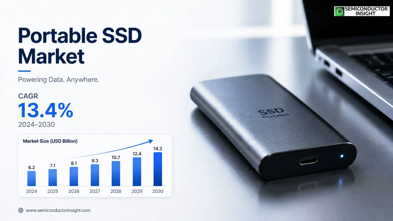
Storage Density Breakthroughs Influencing Portable SSD Market
Portable SSD market sits at the intersection of semiconductor fabrication and consumer data mobility. At its core, every portable SSD is built on NAND flash memory, a technology that has undergone rapid scaling over the last decade. Modern 3D NAND stacks now exceed 200 layers, compared to fewer than 50 layers in early designs, allowing manufacturers to pack terabytes of storage into compact enclosures.
Global semiconductor data from organizations such as the Semiconductor Industry Association indicates that memory chips account for roughly 25-30% of total semiconductor revenue, with NAND flash forming a substantial share. Portable SSDs are a downstream application of this ecosystem, translating wafer-level innovation into real-world storage devices.
Data Volumes Driving Device Relevance
- The rapid growth of data creation is one of the main factors driving portable SSD adoption.
- International Data Corporation estimates that global data generation surpassed 120 zettabytes in 2023 and is expected to exceed 180 zettabytes by 2025.
- As file sizes continue to rise, especially in media production and professional workflows, fast and reliable portable storage has become increasingly important.
For example, a single 4K video project can require 100-500 GB of storage, while professional 8K workflows may exceed 2 TB per project.
- This makes high-speed portable storage a practical necessity rather than a convenience.
- Modern portable SSDs now typically offer storage capacities from 500 GB to 8 TB, sequential read speeds between 500 MB/s and 3,500 MB/s, and interfaces such as USB 3.2, USB4, and Thunderbolt.
- They also use TLC or QLC 3D NAND and controller process nodes ranging from 12 nm to 28 nm. Compared with traditional hard drives, which usually deliver 100-150 MB/s, portable SSDs can be 20-30 times faster, significantly improving performance across industries.
Semiconductor Stack inside a Portable SSD
Host Device → Interface Controller → NAND Flash Controller → 3D NAND Memory → Data Storage Blocks
Each layer is optimized for speed, power efficiency, and thermal management. The controller chip, often fabricated using advanced nodes below 20 nm, manages error correction, wear levelling, and data mapping. Meanwhile, NAND memory uses charge-trap technology to store bits in vertically stacked cells.
Key semiconductor elements include:
- NAND flash dies stacked in multi-layer configurations
- DRAM or DRAM-less controller architectures
- Error correction algorithms such as LDPC (Low-Density Parity Check)
- Power management ICs for thermal and energy efficiency
Interface Speeds and Protocol Evolution
The performance of portable SSDs is closely tied to interface standards, many of which are driven by semiconductor advancements. The shift from USB 3.0 to USB4 has increased bandwidth from 5 Gbps to up to 40 Gbps, enabling near-internal SSD performance in external devices.
Recent real-world examples highlight this shift:
- Newer portable SSDs launched in 2024 support USB 3.2 Gen 2×2, delivering 20 Gbps bandwidth
- Thunderbolt-enabled drives can achieve sustained speeds above 2,800 MB/s
- Gaming consoles and laptops increasingly support direct external SSD expansion
These improvements are not just technical milestones; they redefine how data is moved, edited, and stored across devices.
Manufacturing Scale and Supply Chain Signals
Portable SSD production is closely linked to global NAND output, with industry reports and manufacturer disclosures showing production volumes in the millions of wafers each year. Since each wafer contains thousands of memory dies, the overall scale supports the large and growing demand for portable SSDs worldwide.
A single advanced fabrication facility can process more than 100,000 wafers per month, and each wafer can produce hundreds of gigabytes to terabytes of usable memory. As a result, global portable SSD shipments also reach tens of millions of units annually, based on aggregated shipment disclosures.
NAND fabrication is concentrated in countries such as South Korea, Japan, the United States, and China, while assembly and packaging operations are often carried out in Southeast Asia.
To find out more, feel free to browse our latest updated report: https://semiconductorinsight.com/report/external-portable-ssd-market/
Strategic Developments Gaining Market Pace
The past two years have seen several notable developments:
- Leading storage brands have introduced 8 TB portable SSDs, reflecting higher density NAND adoption
- Semiconductor firms have accelerated QLC NAND deployment, enabling lower cost per gigabyte
- Global chip supply fluctuations in 2022-2023 impacted SSD pricing, with NAND prices dropping by over 30% at certain points, making high-capacity drives more accessible
- Governments, including the United States under the CHIPS and Science Act, are investing billions of dollars in semiconductor manufacturing, indirectly strengthening the NAND supply chain
Advanced Chip Technology Shaping Real World Solutions
Portable SSD Market is a clear example of how semiconductor innovation translates into tangible user benefits. From multi-layer NAND stacks to high-speed controllers, every advancement at the silicon level enhances how individuals and enterprises handle data.
What stands out is the seamless integration of complex semiconductor engineering into a device that fits in a pocket yet can store terabytes of data and transfer it in seconds. This convergence of scale, speed, and efficiency continues to redefine expectations around storage, making portable SSDs one of the most practical outcomes of modern semiconductor progress.

Comments (0)