
Silicon Photonics vs. Pluggable Optics Market 2026: Which Architecture Scales Better?
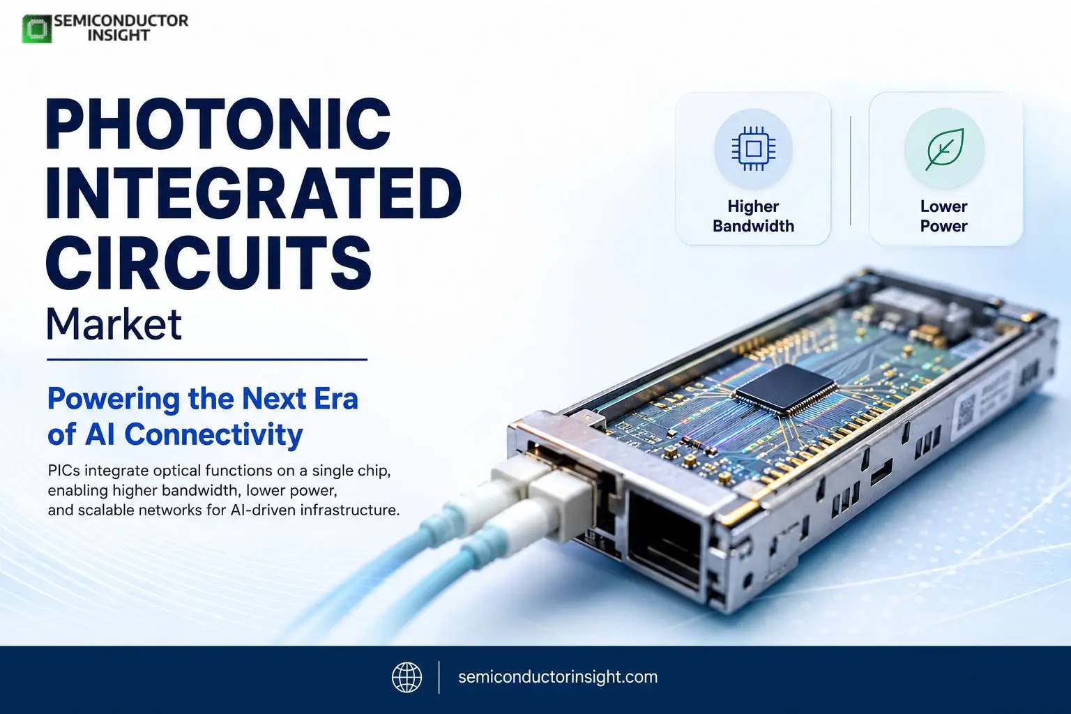
Photonic integrated circuits have moved from a specialist telecom technology into one of the most closely watched segments of the semiconductor industry. As AI training clusters grow from thousands to hundreds of thousands of accelerators, the need for faster, lower-power optical communication has become a central infrastructure challenge. PICs integrate lasers, modulators, waveguides, and photodetectors onto a single chip, replacing many discrete optical components and reducing the energy required to move data across servers and racks.
The timing is significant. Modern AI systems increasingly depend on network performance as much as compute performance. When large language models are trained across massive GPU clusters, every microsecond of latency and every watt of power consumed by interconnects affects total operating cost. This has pushed cloud providers, networking companies, and semiconductor manufacturers to accelerate investment in silicon photonics and related PIC technologies.
Why optical chips are becoming infrastructure?
Traditional copper links struggle as bandwidth requirements climb beyond 400G and 800G. Optical links can carry more data over longer distances with lower signal loss, making them attractive for AI fabrics, cloud networks, and high-performance computing systems.
A practical example is the rapid transition toward 800G optical modules in hyperscale data centers. Industry deployments are already moving beyond 400G, and the roadmap toward 1.6T optical connectivity is gaining momentum. PICs are at the center of this transition because they allow multiple optical functions to be integrated into a compact package that can be manufactured using semiconductor processes.
Why operators are shifting to PICs?
2026 focus
- Higher bandwidth density per rack
- Lower power consumption than equivalent copper links
- Smaller optical module footprints
- Better scalability for AI clusters
- Integration with advanced semiconductor packaging
The AI data center connection
One of the clearest signals comes from the scale of AI infrastructure spending. NVIDIA reported data center revenue of US$115.2 billion for fiscal year 2025, highlighting how rapidly AI networking requirements are expanding. Every large GPU cluster requires an enormous number of optical connections between accelerators, switches, and storage systems.
Cloud operators are increasingly evaluating co-packaged optics, where optical engines are integrated closer to switching silicon. This architecture reduces power consumed by electrical traces and improves overall system efficiency. Several major networking vendors have demonstrated co-packaged optical platforms designed for next-generation AI fabrics, and PIC technology is a foundational element of those designs.
For a more thorough report, please contact us using our most recent report: https://semiconductorinsight.com/report/photonic-integrated-circuits-market/
Manufacturing is entering a new phase
PIC production is increasingly benefiting from the wider semiconductor manufacturing ecosystem, where silicon photonics devices can be built on large silicon wafers using processes that are compatible with advanced CMOS manufacturing. This compatibility supports higher production volumes than many traditional optical assembly methods, making the technology more scalable and efficient.
The sector is also moving closer to mainstream semiconductor operations, with Intel publicly discussing shipments of millions of silicon photonics components for data center applications. At the same time, foundry and packaging providers are expanding their optical integration capabilities, showing that photonics is now being treated as part of the core semiconductor supply chain rather than a standalone specialty segment.
Production Indicators
- Wafer platform: 300 mm silicon
- Manufacturing approach: CMOS-compatible photonics lines
- Optical roadmap: 1.6T class links
- Next-generation focus: AI fabrics
Where the technology is showing up first?
The strongest commercial activity is centered on three key areas. In AI and cloud networking, optical interconnects are used to connect GPU clusters with Ethernet or InfiniBand switches, supporting the growing demand for faster and more efficient data movement. In telecom transport, integrated coherent optics are increasingly used for long-haul and metro fiber networks to improve performance and reliability. High-performance computing is another major area, where low-latency optical fabrics link processors, memory, and storage to handle intensive workloads more effectively.
At the same time, research programs across Europe, North America, and Asia are exploring PICs for sensing, quantum networking, and automotive applications. Even so, AI infrastructure continues to be the main commercial driver at present.
What makes 2026 different?
The most important change is that PICs are no longer being discussed only as a future technology. They are becoming a deployment technology. Hyperscale operators are designing networks around optical scalability, switch vendors are preparing platforms for co-packaged optics, and semiconductor manufacturers are investing in photonic packaging capacity.
In practical terms, photonic integrated circuits market is evolving from a component story into an infrastructure story. The next wave of AI growth will depend not only on more powerful processors, but also on the optical networks that connect them. That shift places PICs alongside advanced packaging, high-bandwidth memory, and accelerator silicon as one of the semiconductor industry’s most strategic technologies.
For readers tracking semiconductor infrastructure, the key question is no longer whether photonic integration will scale, but how quickly optical chips can become a standard building block of every major AI data center.

Comments (0)