
Semiconductor Process Complexity Is Creating New Growth in the Dry Etch Gas
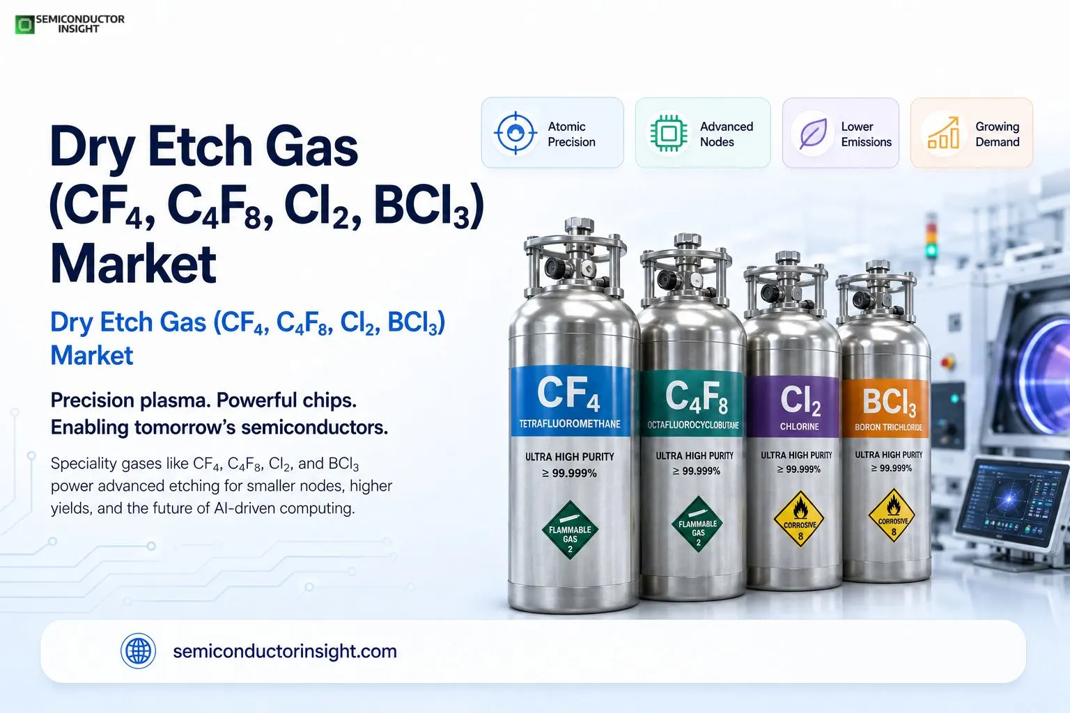
The semiconductor industry is entering a manufacturing phase where precision at the atomic level matters more than ever before. Behind every advanced processor, AI accelerator, and high-bandwidth memory stack lies a highly controlled plasma etching process powered by speciality gases such as CF4, C4F8, Cl2, and BCl3. These gases are no longer viewed as standard industrial consumables. They are now considered strategic materials influencing chip yield, transistor density, and production scalability.
As global semiconductor investments accelerate across the United States, Taiwan, South Korea, Japan, and India, dry etch chemistry is quietly becoming one of the most critical enablers of modern chip fabrication.
Plasma Chemistry Moving Closer to Atomic Precision
- Semiconductor manufacturers are increasingly shifting toward smaller process nodes below 5nm, where plasma etching precision directly affects device performance. Gases like CF4 and C4F8 are widely used in dielectric etching because they help create highly anisotropic structures essential for advanced transistor architectures.
- Meanwhile, chlorine-based gases such as Cl2 and BCl3 are heavily utilised in metal etching applications involving aluminium, tungsten, and compound semiconductor materials. In gallium nitride and silicon carbide device fabrication, chlorine plasma chemistry has become particularly important due to its ability to maintain cleaner sidewalls and tighter dimensional control.
- Taiwan Semiconductor Manufacturing Company reportedly expanded advanced packaging and 3nm production capacities in 2025 to support AI processor demand, increasing the need for highly stable etching chemistries across multiple production stages. Similar expansions are occurring in South Korea and Arizona-based fabs in the United States.
AI Infrastructure Is Increasing Etch Intensity per Wafer
AI chips contain significantly more complex structures compared to earlier consumer processors. High-bandwidth memory integration, chiplet architectures, and 3D stacking require deeper and more intricate etching steps.
A single advanced wafer today may undergo several hundred plasma etching cycles before final packaging. According to semiconductor manufacturing studies published through technical journals and industry engineering conferences, advanced DRAM and NAND fabrication can involve etch depths exceeding 100 micrometres in certain high aspect ratio structures.
- This rising etch intensity per wafer is directly increasing speciality gas consumption volumes across fabs worldwide.
- In 2025, Samsung Electronics and SK hynix continued expanding HBM memory production lines to support AI server deployment. The surge in generative AI infrastructure has consequently pushed demand for fluorocarbon and chlorine-based etch gases used in memory fabrication.
Explore the full report details in our recently refreshed edition anytime: https://semiconductorinsight.com/report/dry-etch-gas-cf-cf-cl-bcl-market/
Environmental Scrutiny Is Reshaping Gas Selection Strategies
CF4 remains effective in plasma processing but is also categorised as a high global warming potential gas. This has created mounting pressure on fabs to improve gas abatement systems and optimise process efficiency.
Some semiconductor manufacturers are now deploying advanced burn-wet scrubber systems capable of reducing perfluorocarbon emissions from etch chambers before atmospheric release. Japan and the European Union are also supporting stricter sustainability frameworks for semiconductor facilities under broader industrial decarbonization initiatives.
Interestingly, this environmental pressure is not reducing dry etch gas demand. Instead, it is accelerating innovation in lower-emission chemistries, recycling systems, and process optimisation software integrated directly into etch tools.
Applied Materials and Lam Research have both highlighted process sustainability improvements in recent semiconductor manufacturing technology updates, particularly around plasma tool efficiency and emission reduction technologies.
Compound Semiconductors Are Creating a New Consumption Layer
- The rise of electric vehicles, renewable power systems, and advanced radar technologies is creating strong momentum for compound semiconductors such as silicon carbide and gallium nitride.
- These materials are harder and chemically different from traditional silicon wafers, requiring specialised dry etch chemistries dominated by chlorine-based gases, including Cl2 and BCl3.
- Global electric vehicle production surpassed 17 million units in 2024, according to international energy data, while silicon carbide wafer investments expanded rapidly across the United States, Germany, Japan, and China. Every new silicon carbide fabrication line creates additional demand for highly selective plasma etching gases and chamber-cleaning chemistries.
- This trend is gradually transforming the dry etch gas ecosystem from a silicon-centric market into a broader advanced materials processing industry.
Geopolitical Semiconductor Policies Are Influencing Gas Supply Chains
The semiconductor supply chain is becoming increasingly regionalised. Governments are now investing billions into domestic chip manufacturing capacity under national security and industrial resilience programs.
The United States CHIPS and Science Act, Japan’s semiconductor revitalisation initiatives, and India’s semiconductor incentive programs are all indirectly supporting speciality gas infrastructure investments.
Large-scale fabs require uninterrupted supplies of ultra-high-purity etch gases with impurity levels controlled down to parts per billion. As a result, industrial gas companies are expanding purification, storage, and localised distribution capabilities near emerging semiconductor clusters.
In Japan, several speciality material suppliers are increasing their focus on semiconductor-grade electronic gases to align with growing domestic and international fab expansion plans.
Equipment Innovation Is Changing Gas Consumption Patterns
Modern plasma etching systems are becoming increasingly software-driven. AI-assisted chamber monitoring, real-time endpoint detection, and predictive maintenance are improving gas utilisation efficiency.
Instead of simply increasing gas flow volumes, fabs are now optimising molecular utilisation rates to reduce waste while maintaining etch uniformity. Some next-generation etch platforms are designed to reduce gas consumption per wafer pass without compromising throughput.
This shift is changing purchasing strategies across semiconductor facilities. Buyers are no longer evaluating gases only on purity and cost. Stability during plasma dissociation, chamber residue formation, and compatibility with advanced EUV processes are becoming equally important selection criteria.
Important Market Information
- Advanced semiconductor fabs can process more than 100,000 wafers per month, significantly increasing speciality gas consumption requirements in plasma etching operations.
- High-bandwidth memory manufacturing used for AI servers expanded sharply in 2025, with major Asian chipmakers increasing HBM production capacity investments.
- CF4 is widely recognised as a high global warming potential gas, prompting semiconductor fabs to adopt advanced abatement systems and emission-control technologies.
- Silicon carbide semiconductor demand is accelerating alongside electric vehicle adoption, which crossed approximately 17 million global EV sales in 2024, according to international energy data.
- Advanced logic and memory manufacturing increasingly require high aspect ratio etching exceeding tens of micrometres, intensifying demand for precision dry etch chemistries.

Comments (0)