

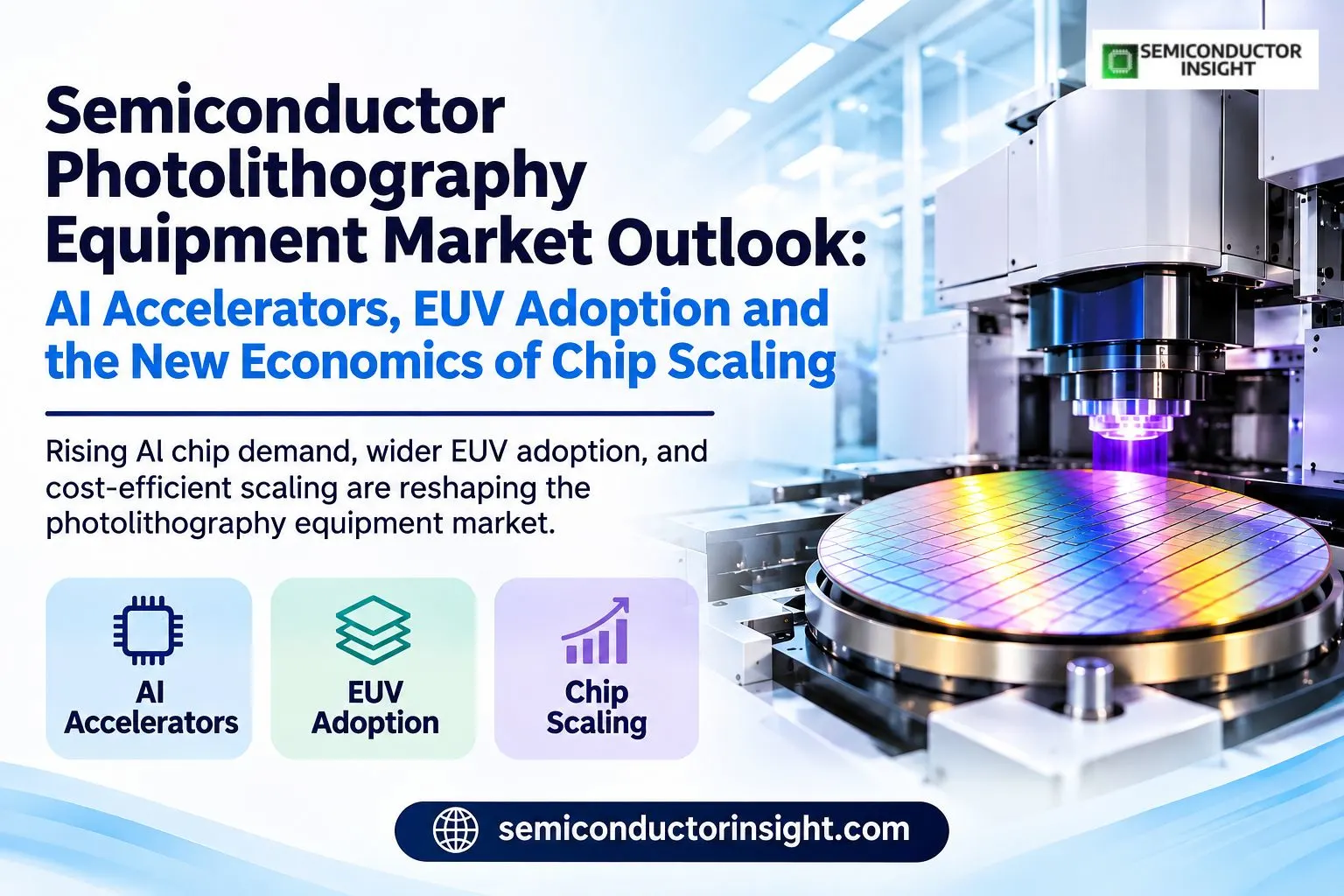
Semiconductor Photolithography Equipment Market Outlook: AI Accelerators, EUV Adoption and the New Economics of Chip Scaling
Semiconductor photolithography equipment sits at the centre of advanced chip manufacturing, translating intricate circuit designs into physical patterns on silicon wafers. The process uses light, masks, photoresists and precision optical systems to create the microscopic structures that allow processors, memory devices and other integrated circuits to function. As chip architectures become denser, lithography equipment is being pushed towards tighter pattern control, improved overlay accuracy and increasingly complex exposure techniques.
- In 2026, the industry is moving beyond conventional scaling. Artificial intelligence processors, high-bandwidth memory and sub-2nm logic are increasing the importance of advanced patterning, while High-NA EUV is beginning to move from technology development towards production use.
High-NA EUV Is Moving from Cleanroom Demonstration to Chip Production
- The most significant development in advanced lithography is the growing industrial readiness of High Numerical Aperture EUV.
- ASML’s High-NA systems use a numerical aperture of 0.55, compared with 0.33 for current-generation EUV platforms. The higher optical resolution is designed to print smaller features and reduce reliance on multiple patterning steps for selected layers.
- A major milestone arrived in July 2026 when Intel Foundry began using High-NA EUV for selected layers in a subset of its Core Ultra Series 3 processors based on the Intel 18A process.
- By September, Intel and ASML reported that more than 1 million wafers had been processed across certification, research, testing and selected production activities.
- This is an important step because it demonstrates that the technology is being evaluated under manufacturing conditions rather than remaining confined to laboratory research.
AI Chip Complexity Is Changing the Economics of Lithography
The expansion of AI accelerators and high-performance computing is increasing demand for advanced logic and memory devices. These chips require intricate transistor structures, dense interconnects and highly controlled pattern placement. Photolithography equipment must therefore deliver more than smaller printed dimensions: it must maintain overlay precision, process stability and productive wafer throughput across increasingly complex manufacturing sequences.
ASML’s October 2026 quarterly results provide a clear indication of equipment demand. The company reported 113 new lithography systems sold in Q3 2026, compared with 86 in Q2. Quarterly net sales reached €11.7 billion, while installed-base service and field-option sales contributed approximately €3.3 billion. ASML also raised its full-year 2026 sales outlook to €44–45 billion, citing strong customer demand, particularly associated with AI investment.
Twelve-Inch Photomasks Could Reshape the High-NA Production Roadmap
A significant development announced by ASML and TSMC in September 2026 is the proposed transition towards 12-inch photomasks for High-NA EUV. The semiconductor industry has traditionally relied on 6-inch photomasks, but larger formats could improve scanner productivity and reduce stitching constraints.
The initiative targets a 12-inch mask pilot line by 2031, with the objective of supporting advanced-node High-NA production readiness by 2033. TSMC has indicated that it intends to use High-NA technology in high-volume manufacturing for advanced nodes from 2030. This collaboration highlights how lithography progress depends on more than scanner development: masks, materials, inspection systems and manufacturing processes must evolve together.
A Brief Look at Our Detailed Analysis Related Report: https://semiconductorinsight.com/report/semiconductor-photolithography-equipment-market/
The Angstrom Era Is Creating a New Research Environment
- Research organisations are helping equipment manufacturers and chipmakers prepare for future patterning requirements.
- In March 2026, imec announced the arrival of ASML’s EXE:5200 High-NA EUV system in its cleanroom. The platform is intended to support research into sub-2nm logic and high-density memory technologies, with qualification targeted for the fourth quarter of 2026.
- The significance extends beyond the scanner itself. Advanced lithography requires coordinated development of photoresists, photomasks, metrology, defect inspection and process integration.
- Research facilities such as imec provide an environment where these technologies can be tested together before wider industrial deployment.
India’s Semiconductor Expansion Is Adding a New Equipment Dimension
India’s emerging chip manufacturing ecosystem is creating additional opportunities for semiconductor equipment suppliers. In May 2026, Tata Electronics and ASML announced a strategic partnership supporting India’s Dholera semiconductor fabrication project. The collaboration covers lithography tools, workforce development, research and supply-chain development.
This is important because a new fabrication facility requires more than the installation of production equipment. It needs process engineers, maintenance capabilities, cleanroom infrastructure, materials suppliers and long-term technical support. Lithography equipment partnerships can therefore contribute to the development of a broader domestic manufacturing ecosystem.
Precision, Productivity and Process Integration Will Define the Next Phase
Semiconductor Photolithography Equipment Market is entering a period in which the competitive value of a scanner will increasingly depend on its integration with the wider fabrication process. High-NA EUV, larger photomasks, advanced resists and improved metrology are becoming interconnected priorities. At the same time, established DUV and conventional EUV systems will remain essential for manufacturing many chip layers and mature-node devices.
The next stage of progress will depend on how effectively manufacturers balance resolution, throughput, reliability and total production cost. As AI computing expands and chip architectures become more demanding, photolithography equipment will remain one of the most strategically important technologies in the global semiconductor supply chain.

Comments (0)