Market Insights
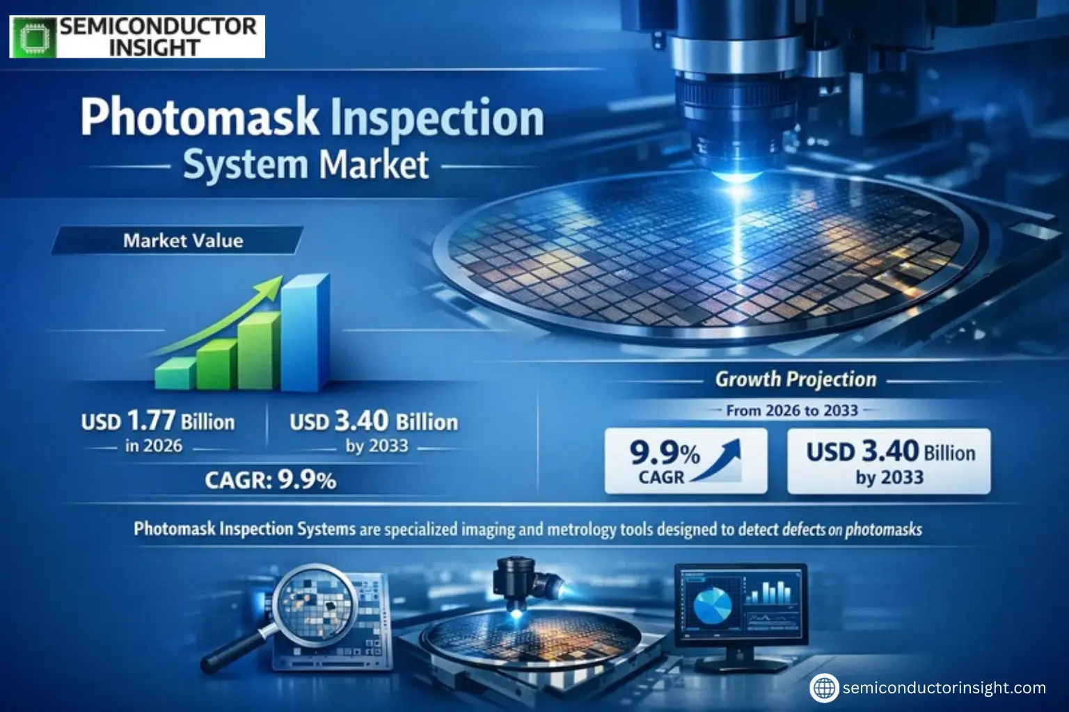
Global Photomask Inspection System Market was valued at USD 1.77 billion in 2026 and is projected to reach USD 3.40 billion by 2033, exhibiting a CAGR of 9.9% during the forecast period.
Photomask Inspection Systems are specialized imaging and metrology tools designed to detect defects on photomasks with high precision. These systems play a critical role in semiconductor manufacturing by identifying imperfections that could impact lithography quality and yield. The technology enables detailed analysis of defect type, size, location, and printability, supporting decisions on repair or process adjustments.
The market growth is driven by increasing demand for advanced semiconductor nodes, where tighter defect tolerances become essential. The adoption of EUV lithography further amplifies the need for sophisticated inspection solutions as mask complexity rises. Key industry players such as KLA Corporation, Lasertec, and Applied Materials continue to innovate in this space, focusing on higher resolution capabilities and improved throughput to meet evolving industry requirements.
MARKET DRIVERS
Growing Semiconductor Industry Demand
The increasing demand for advanced semiconductor devices is driving the Photomask Inspection System Market. With semiconductor manufacturers pushing for smaller node sizes (below 7nm), the need for high-precision photomask inspection has become critical. The market is projected to grow at 7.2% CAGR through 2028 as foundries expand production capacity.
Advancements in EUV Lithography
Extreme Ultraviolet (EUV) lithography adoption requires more sophisticated photomask inspection systems capable of detecting nanometer-scale defects. Leading manufacturers are investing heavily in systems with higher resolution capabilities (below 15nm sensitivity) to keep pace with technology nodes at 3nm and below.
Photomask complexity continues to increase, with multi-patterning techniques driving 42% more inspection steps per mask compared to traditional processes.
MARKET CHALLENGES
High System Costs and ROI Pressures
Advanced photomask inspection systems carry price tags exceeding USD 10 million, creating significant capital expenditure challenges for smaller manufacturers. The average payback period has extended to 3-4 years due to rapid technological obsolescence.
Other Challenges
Defect Detection Complexity
As pattern sizes shrink below 10nm, distinguishing actual defects from noise requires increasingly sophisticated algorithms, pushing computational requirements beyond current hardware capabilities in some systems.
Throughput Limitations
High-resolution inspection systems currently average 5-7 wafers per hour, creating bottlenecks in high-volume manufacturing environments that process thousands of wafers daily.
MARKET RESTRAINTS
Concentration of Technical Expertise
The highly specialized nature of photomask inspection systems creates significant barriers to entry. Only five companies worldwide currently possess the R&D capabilities to develop cutting-edge inspection solutions, limiting market competition.
MARKET OPPORTUNITIES
AI-Powered Inspection Solutions
Machine learning applications in photomask inspection systems offer 30-40% improvement in defect classification accuracy while reducing false positives. This technology is becoming critical for advanced nodes where human verification becomes impractical.
Photomask Inspection System Market Trends
Rising Demand Driven by Advanced Semiconductor Nodes
Global Photomask Inspection System Market is projected to grow from USD 1765 million in 2026 to USD 3400 million by 2033 at a 9.9% CAGR, driven by increasing complexity in semiconductor manufacturing. As chipmakers transition to nodes below 7nm, defect tolerances tighten, requiring more advanced inspection capabilities. EUV lithography adoption further amplifies demand, with photomasks becoming critical yield-limiting factors.
Other Trends
Technology Advancements
Modern photomask inspection systems now incorporate AI-driven defect classification, higher resolution imaging (sub-20nm), and improved correlation with wafer printing behavior. Leading suppliers are integrating these capabilities with workflow automation to reduce false positives and accelerate mask requalification cycles by 30-40% compared to previous generations.
Regional Market Shifts
Asia dominates with 68% market share in 2026, led by semiconductor hubs in Taiwan, South Korea and China. North America and Europe maintain strong positions in advanced R&D applications, particularly for EUV mask inspection. The Middle East is emerging as a growth region with new semiconductor fabrication investments in the UAE and Israel.
Supply Chain Dynamics
The industry maintains 40-60% gross margins but faces component shortages in precision optics and motion control systems. Vendors are establishing strategic partnerships with subsystem suppliers to secure critical components like high-sensitivity detectors and vibration isolation platforms.
Competitive Landscape Evolution
Lasertec and KLA collectively hold over 55% market share, leveraging their expertise in wafer and mask inspection. New entrants from China (Yuweitek, TENYUM) are gaining traction in mature nodes, challenging established players with cost-optimized solutions. The market sees increasing vertical integration as inspection system providers acquire mask repair and data analytics capabilities.
COMPETITIVE LANDSCAPE
Key Industry Players
Innovation and Precision Drive Photomask Inspection System Market Competition
Photomask Inspection System Market is dominated by Lasertec and KLA Corporation, which collectively account for over 60% of the global market share. These industry leaders differentiate through advanced electron beam inspection technologies and AI-powered defect classification systems optimized for EUV photomasks. Both companies maintain strong R&D pipelines with significant reinvestment of their 45-55% gross margins into next-generation inspection solutions.
Niche players like NuFlare Technology and Carl Zeiss specialize in optical inspection solutions for mature nodes, while emerging Chinese manufacturers focus on cost-competitive alternatives for domestic semiconductor fabs. The market also features specialized providers like MueTec and VPtek offering inspection systems tailored for specific applications such as flat panel displays or advanced packaging.
List of Key Photomask Inspection System Companies Profiled
- Lasertec Corporation
- KLA Corporation
- Applied Materials
- NuFlare Technology
- Advantest Corporation
- Carl Zeiss AG
- MueTec GmbH
- LAZIN Inc.
- VPtek
- Yuweitek
- TENYUM
- Holon Co., Ltd.
- Vision Technology
- Multiprobe Incorporated
- Leica Microsystems
Segment Analysis:
| Segment Category | Sub-Segments | Key Insights |
| By Type |
|
Mask Pattern Defect Detection Equipment dominates as wafer shrinks demand nanometer-level defect identification:
|
| By Application |
|
Semiconductor Industry represents the primary growth driver with distinct requirements:
|
| By End User |
|
Semiconductor Fabs exhibit strongest adoption momentum:
|
| By Substrate Material |
|
Quartz Glass Substrate inspection remains technologically demanding:
|
| By Technology |
|
Hybrid Systems are gaining strategic importance:
|
Regional Analysis: Photomask Inspection System Market
Taiwan’s photomask inspection market thrives due to its dense semiconductor manufacturing base, particularly for leading-edge nodes. The country’s pure-play foundry model necessitates frequent mask inspections to maintain yield rates at advanced technology nodes. Domestic mask shops collaborate closely with inspection system suppliers to develop customized solutions.
Japan maintains a strong position in photomask inspection technologies through its specialty equipment manufacturers. Japanese companies lead in developing mask inspection solutions for EUV lithography and multi-patterning applications. The country’s focus on quality control drives demand for high-precision inspection systems.
South Korea’s photomask inspection market is influenced by its dominance in memory chip production. The country’s large-scale memory fabs require specialized mask inspection solutions optimized for high-volume production environments. Local semiconductor giants invest heavily in inspection technologies to maintain competitive yields.
China’s photomask inspection system demand grows with its semiconductor self-sufficiency initiatives. New fabrication facilities across China are driving sales of both advanced and mature-node inspection equipment. Domestic equipment makers are gaining traction while foreign suppliers maintain technology advantages in key segments.
North America
North America’s photomask inspection system market benefits from strong R&D activities and proximity to major IC design companies. The region specializes in advanced inspection solutions for emerging technologies, with semiconductor equipment vendors collaborating closely with research institutions. California’s Silicon Valley remains a hub for prototyping next-generation inspection technologies, while Arizona’s expanding fab capacity creates new demand. The market features a mix of captive mask shops and merchant suppliers investing in sub-nanometer defect detection capabilities.
Europe
Europe maintains a specialized position in the photomask inspection system market through its expertise in niche semiconductor applications. The region excels in inspection solutions for automotive and industrial chips, emphasizing reliability and safety-critical applications. Germany and France host several equipment innovators developing customized inspection technologies. Europe’s collaborative research programs drive advancements in mask inspection for new materials and packaging technologies.
Middle East & Africa
The Middle East is emerging as a new market for photomask inspection systems through strategic investments in semiconductor manufacturing. National initiatives in Saudi Arabia and the UAE aim to build local semiconductor capabilities, creating opportunities for equipment suppliers. Africa’s market remains nascent but shows potential growth as regional electronics manufacturing expands.
South America
South America’s photomask inspection system market centers on Brazil’s modest but growing semiconductor activities. The region primarily serves local electronics manufacturing needs with mature-node inspection solutions. While market size remains limited compared to other regions, localization incentives are driving gradual infrastructure development.
Report Scope
This market research report provides a comprehensive analysis of the Photomask Inspection System Market , covering the forecast period 2026–2033. It offers detailed insights into market dynamics, technological advancements, competitive landscape, and key trends shaping the industry.
Key focus areas of the report include:
- Market Overview: The report begins with an overview outlining its current market scenario, key growth indicators, and industry transformation drivers. It discusses macroeconomic factors, demand–supply balance, regulatory landscape, and the strategic role of semiconductors in powering advancements across industries such as automotive, telecommunications, consumer electronics, and industrial automation.
- Market Size & Forecast: Historical data and future projections for revenue, unit shipments, and market value across major regions and segments.
- Segmentation Analysis: Detailed breakdown by product type, technology, application, and end-user industry to identify high-growth segments and investment opportunities.
- Regional Insights: Insights into market performance across North America, Europe, Asia-Pacific, Latin America, and the Middle East & Africa, including country-level analysis where relevant.
- Competitive Landscape: Profiles of leading market participants, including their product offerings, R&D focus, manufacturing capacity, pricing strategies, and recent developments such as mergers, acquisitions, and partnerships.
- Technology Trends & Innovation: Assessment of emerging technologies, integration of AI/IoT, semiconductor design trends, fabrication techniques, and evolving industry standards.
- Market Drivers & Restraints: Evaluation of factors driving market growth along with challenges, supply chain constraints, regulatory issues, and market-entry barriers.
- Stakeholder Insights: Insights for component suppliers, OEMs, system integrators, investors, and policymakers regarding the evolving ecosystem and strategic opportunities.
Primary and secondary research methods are employed, including interviews with industry experts, data from verified sources, and real-time market intelligence to ensure the accuracy and reliability of the insights presented.
FREQUENTLY ASKED QUESTIONS:
What is the current market size of Photomask Inspection System Market?
-> Photomask Inspection System Market was valued at USD 1.77 billion in 2026 and is projected to reach USD 3.40 billion by 2033, exhibiting a CAGR of 9.9% during the forecast period.
What is the growth rate of Photomask Inspection System Market?
-> The market is expected to grow at a CAGR of 9.9% during the forecast period (2026-2033).
Which key companies operate in Photomask Inspection System Market?
-> Key players include Lasertec, KLA, Applied Materials, NuFlare Technology, Advantest, Carl Zeiss, MueTec, LAZIN, VPtek, Yuweitek, and TENYUM.
What are the key growth drivers?
-> Key growth drivers include tighter defect tolerance requirements, increasing mask complexity, expansion of EUV usage, and demand for fast defect confirmation in semiconductor manufacturing.
Which segment dominates the market by application?
-> The Semiconductor Industry segment holds the largest market share due to growing adoption of advanced patterning technologies.
Which region dominates the market?
-> Asia is the dominant market, with significant contributions from China, Japan, and South Korea, owing to strong semiconductor manufacturing presence.

Get Sample Report PDF for Exclusive Insights
Report Sample Includes
- Table of Contents
- List of Tables & Figures
- Charts, Research Methodology, and more...