
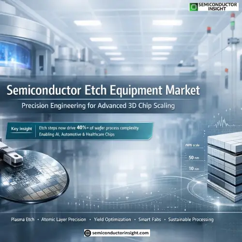
Semiconductor Etch Equipment Market Developments Signal Long-Term Opportunity across Precision Manufacturing
Semiconductor etch equipment sits at the heart of modern chip making. While consumers see smartphones, AI servers, and medical wearable, the real breakthroughs happen deep inside fabrication plants where silicon is shaped layer by layer. Etching is the process that removes material with extreme accuracy, forming the microscopic patterns that define chip performance.
As semiconductor structures become more complex, the importance of etch precision has grown dramatically. This market is no longer just about removing material it is about enabling the next era of digital infrastructure, from cloud computing to healthcare monitoring systems.
Etch equipment is one of the most critical enablers of advanced semiconductor scaling.
Why Etching Matters More in the Era of 3D Architectures?
The semiconductor industry has shifted beyond flat transistor designs. Today, manufacturers are building 3D NAND memory, gate-all-around transistors, and multilayer logic stacks. These architectures require etching solutions that can operate with near-perfect uniformity at nanometre scale.
In this environment, even the smallest deviation can impact yield and device reliability. That is why leading fabs are investing heavily in high-performance etch platforms capable of handling:
- Atomic-level feature definition
- High-aspect-ratio etching for vertical structures
- Reduced defect generation for tighter geometries
The market’s growth is closely tied to the continued move toward smaller nodes and taller structures.
Demand Expansion Driven by AI, Automotive, and Healthcare Chips
Etch equipment demand is rising because chip demand itself is broadening. AI acceleration chips, automotive semiconductors, and connected healthcare devices all require advanced manufacturing steps.
In healthcare, etching plays a role in producing chips used for:
- Diagnostic imaging systems
- Implantable medical electronics
- Wearable health trackers
As healthcare systems increasingly adopt connected devices, semiconductor production requirements expand in parallel. Medical-grade electronics are becoming a major downstream demand contributor.
Process Innovation: Plasma, Dry Etch, and Atomic Layer Precision
Modern etch systems are built around plasma-based dry etching, which provides much greater control than wet chemical methods. The industry is also moving toward atomic layer etching, where removal occurs one layer at a time.
This innovation focus is driven by the need for:
- Higher selectivity, meaning only the intended layer is etched
- Improved sidewall control for sharper pattern transfer
- Lower contamination risk inside ultra-clean fab environments
- Equipment makers are also integrating AI-driven process monitoring to reduce variability and boost throughput.
To Stay Tuned with More meaningful and In-Depth Related Insights, Do Visit here:
https://semiconductorinsight.com/report/semiconductor-etch-equipment-market/
Statistical Signals Shaping the Market
Several measurable trends highlight the market’s direction:
- Advanced etch steps now account for over 40% of total wafer process complexity in cutting-edge fabs.
- Leading-edge fabs can require double-digit increases in etch tool installations when moving from planar to 3D architectures.
- Yield improvement programs in major foundries have shown 10-15% efficiency gains when process control software is integrated into etch workflows.
These indicators show how etch equipment is becoming both a volume driver and a precision differentiator.
Supply Ecosystem Pressures and Component Dependencies
Etch equipment manufacturing depends on highly specialized subsystems, including vacuum chambers, RF power modules, and advanced ceramics. Supply constraints in these areas can influence delivery cycles for fab expansions.
At the same time, fabs are pushing for more localized tool supply strategies to reduce exposure to global disruptions. The market is increasingly shaped by:
Sustainability and Resource Efficiency in Etch Processes
Sustainability is emerging as a serious theme in semiconductor manufacturing. Etch processes consume gases and energy, and fabs are under pressure to reduce emissions and improve resource efficiency.
New systems are being designed with:
- Lower global warming potential gas alternatives
- Improved chamber cleaning efficiency
- Energy optimization through smart plasma tuning

Comments (0)