
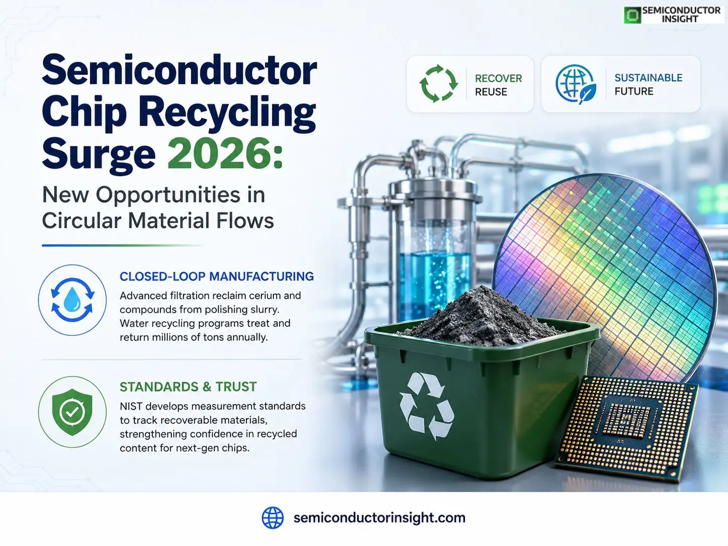
Semiconductor Chip Recycling Surge 2026: New Opportunities in Circular Material Flows
Semiconductor circular economy practices are gaining momentum as manufacturers seek ways to recover valuable materials from end-of-life electronics and production scraps. These efforts focus on closing loops for silicon wafers, rare earth elements, and precious metals that power modern chips, reducing reliance on virgin mining while addressing growing e-waste volumes.
Material Recovery Pathways Reshaping Production Cycles
In wafer fabrication plants, chemical mechanical polishing generates substantial slurry waste containing cerium and other compounds. Facilities now deploy advanced filtration systems to reclaim these for reuse, cutting freshwater consumption and lowering disposal costs. TSMC has implemented water recycling programs that treat and return millions of tons of process water annually, demonstrating how closed-loop systems operate at scale in high-volume manufacturing.
Government-supported initiatives like the U.S. NIST Circular Economy Program develop measurement standards for tracking recoverable materials across supply chains. This work supports confidence in recycled content performance for next-generation chips used in data centers and electric vehicles.
Key Material Flow Stages
- Collection of end-of-life devices and fab scraps
- Dismantling and sorting of components
- Chemical or thermal extraction of metals
- Purification and qualification for new wafer production
Rare Earth Recovery from Discarded Electronics
Rare earth elements like neodymium, gallium, and germanium appear in small quantities within semiconductors but prove critical for performance. Traditional mining dominates supply, yet recycling from hard drives, servers, and consumer gadgets offers a domestic alternative.
Partnerships such as those between ERI and ReElement Technologies process discarded electronics to extract refined rare earth oxides. One pilot recovered materials from thousands of pounds of shredded hard disk drives, achieving high purity rates suitable for new magnet and chip applications. Western Digital and Microsoft collaborations have similarly targeted data center equipment, yielding measurable volumes of reusable elements.
U.S. EPA data from earlier assessments showed consumers and businesses discarding around 2.37 million tons of electronics in 2009, with only a fraction recycled at that time. Updated flows indicate persistent challenges, with global e-waste generation reaching tens of millions of tons yearly according to UN monitoring.
You can freely browse our most recent updated report to learn more about it before scrolling further: https://semiconductorinsight.com/report/semiconductor-circular-economy-market/
Policy Frameworks Supporting Closed-Loop Systems
- The CHIPS and Science Act in the United States authorizes substantial funding for domestic semiconductor research and manufacturing, explicitly incorporating recycling and materials efficiency goals. This includes efforts to improve energy use and chip recycling in new facilities. New York State’s Green CHIPS program offers incentives for environmentally conscious projects, attracting investments that integrate circular practices from the outset.
- In Europe, the Circular Economy Action Plan sets targets for secondary raw materials, influencing how semiconductor firms design products for easier disassembly and material recovery. Programs like REE4EU explore metallurgical processes to reclaim rare earths from industrial residues and end-of-life items through energy-efficient methods.
Water and Chemical Reuse In Fabrication Plants
Semiconductor manufacturing consumes enormous quantities of ultra-pure wateroften thousands of liters per wafer. Circular approaches treat wastewater on-site for reuse, with some advanced nodes achieving recovery rates that significantly reduce intake from municipal supplies. Intel has documented successes in reclaiming chemicals and solvents, feeding them back into production lines and minimizing environmental discharge.
These practices extend beyond individual plants. Industry-wide collaborations develop shared standards for material passports that track composition and recyclability, easing integration of reclaimed content into new supply chains.
Volume Highlights from Public Reports
- U.S. e-waste generation exceeded 7 million tons in recent tallies, with collection varying by state programs
- Global documented formal recycling captured only a portion of total flows, leaving substantial recoverable metals untapped
- Individual facilities report reclaiming hundreds of tons of process byproducts yearly through targeted programs
Design Innovations Enabling Higher Circularity
Chip designers now consider end-of-life scenarios during the layout phase. Modular architectures in advanced packages facilitate component harvesting, while standardized materials simplify sorting at recycling centers. Framework’s work on repairable electronics, in partnership with semiconductor suppliers, highlights how upgradable designs extend product life and improve recovery economics.
In data centers, operators implement asset tracking to route decommissioned servers into certified recovery streams rather than landfills. This preserves embedded gold, copper, and specialty metals for subsequent use.
Global Collaboration Examples Advancing Progress
Asian manufacturing leaders like TSMC partner with environmental ministries on technologies for reclaiming resources from production waste. European projects emphasize urban miningextracting materials above ground from accumulated electronics stockpiles.
U.S. Department of Defense investments target recovery of critical elements for defense applications, supporting dual-use advancements that benefit commercial semiconductor lines. These cross-border and public-private efforts build resilience against supply disruptions while advancing sustainability metrics.
Scaling Challenges and Technical Breakthroughs
Flash Joule heating techniques from research labs, such as at Rice University, show promise for rapid extraction of rare earths from mixed waste streams with lower energy input than traditional hydrometallurgy. Bioleaching using microorganisms offers another gentle pathway under exploration for selective metal recovery.
As AI and high-performance computing drive chip demand higher, circular systems help balance growth with resource constraints. Facilities incorporating these methods report operational efficiencies alongside environmental gains, creating models that others in the ecosystem can adapt.
The semiconductor circular economy continues expanding through practical implementations at plants worldwide, policy backing from authorized programs, and innovations that turn yesterday’s devices into tomorrow’s wafers. This shift supports more resilient supply chains and responsible material stewardship across the technology landscape.

Comments (0)