
Quartz Materials for Semiconductor Market vs. Ceramic Process Materials Where Each Fits
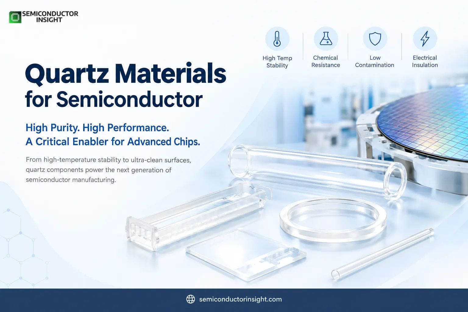
A semiconductor wafer may receive most of the attention, but the manufacturing environment surrounding it is built from materials that must remain stable under extreme temperatures, reactive chemicals and repeated processing cycles. Quartz is one of those quiet enabling materials. Tubes, boats, rings, liners, plates and other fused-quartz components routinely operate inside equipment used for wafer processing, diffusion, oxidation, and deposition and cleaning.
As semiconductor manufacturing moves toward more advanced nodes, larger wafers and increasingly complex process sequences, the requirements placed on these components are becoming more demanding.
Why Quartz Earned a Place inside the Fab?
- Quartz, primarily silicon dioxide (SiO₂), is valued in semiconductor processing because of its combination of high-temperature stability, chemical resistance, electrical insulation and comparatively low contamination potential.
- Fused quartz can withstand temperatures around 1,000°C and above depending on grade and application, while high-purity varieties are engineered specifically to minimize metallic and particulate contamination.
- That matters because microscopic contamination introduced during processing can affect device yield.
- The material therefore appears in process hardware rather than simply as a structural material. Its role can extend across wafer carriers, reaction tubes, liners, boats, rings and other components exposed to process environments.
The 300 mm Transition Is Changing Component Requirements
The semiconductor industry’s move toward 300 mm wafers has increased the physical scale and precision requirements of wafer-processing hardware. A 300 mm wafer has a diameter of approximately 11.8 inches, compared with about 7.9 inches for a 200 mm wafer.
That difference is significant for quartz components because larger wafers require larger process chambers, carriers and supporting structures while maintaining extremely tight dimensional tolerances.
- SEMI reported that global silicon wafer shipments reached 12,742 million square inches in 2025, compared with 12,317 million square inches in 2024. The organization also reported that 300 mm wafers represented the dominant shipment category by area.
This creates a direct connection between wafer production volumes and the recurring requirement for high-purity process components.
Inside the Quartz Process Chain
The role of quartz can be understood through a simplified manufacturing path:
High-Purity Silica Feedstock → Fused Quartz Production → Precision Fabrication → Cleaning → Inspection → Semiconductor Equipment Integration → Wafer Processing
Each stage matters because semiconductor-grade quartz cannot simply be treated like ordinary industrial glass. Fabricators must control geometry, surface condition, contamination, thermal behavior and particle generation.
Where the Material Meets the Wafer
- Quartz components are particularly visible in thermal processing environments. Quartz boats can hold wafers during furnace processing, while quartz tubes form part of the controlled process environment.
- In oxidation and diffusion processes, the component may experience elevated temperatures and reactive atmospheres for extended periods.
- The combination of heat and chemical exposure makes material purity and surface quality particularly important.
- For plasma-based processes, quartz can also be used where electrical insulation and resistance to particular process chemistries are required, although the appropriate material depends heavily on the specific chamber environment.
Purity Is Becoming a Manufacturing Specification
The semiconductor industry operates at contamination levels that would be insignificant in most conventional manufacturing environments. A particle that is invisible to the naked eye can potentially become a yield issue when it reaches a sensitive wafer surface.
This is why semiconductor-grade quartz production involves specialized cleaning and inspection procedures. Manufacturers may evaluate trace metallic impurities, surface particles, dimensional accuracy and microscopic defects before components enter semiconductor equipment.
- The critical metric is therefore not simply whether a quartz part survives a process cycle. It is whether it can repeatedly survive the process without becoming a source of contamination or dimensional instability.
To find out more, feel free to browse our latest updated report: https://semiconductorinsight.com/report/quartz-materials-for-semiconductor-market/
AI Chips Are Quietly Increasing the Importance of Process Hardware
The rapid expansion of AI accelerators, high-bandwidth memory and advanced logic is pushing semiconductor manufacturers to add or upgrade fabrication capacity. TSMC, for example, has continued expanding advanced manufacturing capacity while reporting strong demand associated with AI-related applications. Its 2025 annual reporting highlighted continued investment in advanced technologies and manufacturing capacity.
More wafer-processing capacity ultimately means more process equipment, replacement parts and consumable components. Quartz therefore participates in the semiconductor expansion indirectly: it is part of the physical infrastructure required to repeatedly process wafers.
The Shift toward Smarter Quartz Component Engineering
- The next development is not simply producing more quartz.
- Component manufacturers are increasingly focusing on longer service life, tighter tolerances, improved surface finishing and more controlled cleaning processes.
- For fabs, this can translate into fewer particle-related problems, more predictable maintenance cycles and greater consistency across high-volume manufacturing.
Quartz may not determine transistor architecture, gate design or chip performance directly. Yet every wafer passes through an ecosystem of equipment and materials that must operate reliably around those technologies.
As semiconductor manufacturing becomes more complex, high-purity quartz is increasingly being treated as precision process hardware rather than an ordinary consumable material.

Comments (0)