

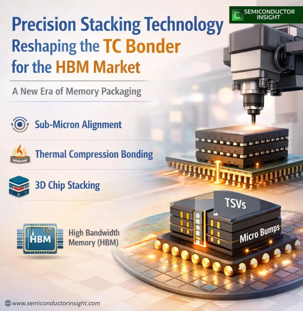
Precision Stacking Technology Reshaping the TC Bonder for HBM Market
A New Era of Precision Memory Packaging
The world of advanced computing is entering a phase where memory performance defines processing power. As artificial intelligence systems demand faster data transfer and ultra-low latency, High Bandwidth Memory HBM has emerged as a foundational technology. At the center of this transformation stands the TC Bonder for HBM Market, a highly specialized semiconductor packaging segment focused on achieving ultra-precise chip stacking and electrical interconnection.
In contrast to traditional bonding methods, semiconductor makers may stack several DRAM dies with remarkable structural stability and alignment accuracy thanks to thermal compression bonding. This capability is essential for modern AI accelerators, GPUs, and data-intensive computing architectures where performance depends on compact and high-speed memory structures. The increasing complexity of chip architecture is steadily pushing TC bonder technology toward higher precision, improved thermal stability, and automation-driven manufacturing processes.
Thermal Compression Bonding Technology Insights
The TC bonder operates through a controlled process that combines heat, pressure, and alignment control to create robust electrical connections between stacked memory chips. This process forms micro-scale interconnects that support high data transfer speeds and improved signal reliability.
Modern TC bonding systems use advanced positioning systems capable of sub-micron alignment precision, ensuring reliable stacking even in extremely dense memory architectures. The technology supports 3D stacking, enabling vertical integration of memory layers while maintaining minimal footprint and improved bandwidth efficiency.
The process typically involves the use of Non-Conductive Film NCF, micro bumps, and Through Silicon via TSV structures that facilitate electrical communication between layers. These elements create stable bonding interfaces and help improve device durability under high thermal loads.
As semiconductor packaging evolves from traditional wire bonding toward advanced 3D integration, TC bonding has become a preferred method for high-performance memory production due to its ability to support miniaturization and high reliability.
HBM Architecture and Chip Stacking Innovation
HBM manufacturing depends heavily on vertical stacking technology. Memory dies are layered one above another and interconnected through TSV channels, enabling extremely fast communication between processor and memory.
TC bonders ensure the structural integrity of these stacks by maintaining precise pressure and temperature conditions during bonding. This precision allows manufacturers to produce multi-layer memory stacks exceeding 12 or even 16 layers, supporting higher storage capacity and faster processing performance.
Advanced HBM generations now deliver significantly improved speed and energy efficiency compared to previous memory architectures. These improvements make TC bonding technology indispensable for next-generation computing systems, particularly those used in machine learning and data centre environments.
The shift toward higher stack density also increases the complexity of packaging, requiring improved process control, enhanced thermal management, and more accurate bonding systems.
Feel Free to Reach Our Most Recent Updates of the Report: https://semiconductorinsight.com/report/tc-bonder-for-hbm-market/
Material Science and Process Chemistry in TC Bonding
- The effectiveness of TC bonding relies heavily on material engineering and chemical process control. Several material systems play a critical role in achieving reliable bonding performance.
- Non-Conductive Film NCF acts as an insulating adhesive that ensures mechanical stability while preventing electrical short circuits. Its chemical composition supports thermal resistance and maintains bonding strength under high operational stress.
- Flux materials assist in surface preparation by removing oxidation and improving metal-to-metal contact during bonding. Meanwhile, underfill materials enhance structural integrity and protect bonded layers from mechanical damage.
- Temperature control within the bonding chamber is equally important. Bonding typically occurs under elevated temperature ranges to activate diffusion processes at the interface, ensuring strong interconnect formation.
- Continuous innovation in polymer chemistry and adhesive technology is enabling faster bonding cycles, higher yield rates, and improved reliability in semiconductor packaging.
Integration with AI and High Performance Computing Systems
The rapid expansion of artificial intelligence infrastructure has significantly increased demand for high-performance memory solutions. TC bonders support the production of HBM modules used in AI processors, cloud computing hardware, and high-end graphics systems.
Advanced semiconductor packaging now integrates TC bonding with 2.5D packaging, chiplet architecture, and heterogeneous integration technologies. These innovations enable compact system design and improved processing efficiency.
As AI workloads continue to scale, memory bandwidth requirements are increasing rapidly, positioning TC bonding as a critical enabler of next-generation computing performance.

Comments (0)