Key Statistics
Key Takeaways
- TC-MUF is the leading bonder type because molded-underfill HBM assembly provides strong mechanical support, thermal performance and production maturity for high-layer memory stacks.
- HBM3/3E is the current revenue-leading application, driven by AI accelerators and high-performance computing, while HBM4 is the major equipment-upgrade opportunity through tighter pitch and higher stack complexity.
- Memory manufacturers are the largest end-user group because HBM production is concentrated among vertically integrated DRAM suppliers with large capital programs and tight process control.
- Asia Pacific is the dominant regional market, led by South Korea, Taiwan and Japan through memory manufacturing, advanced packaging, equipment engineering and OSAT capacity.
- Bonding technology is moving toward fluxless TCB and hybrid bonding. ASMPT introduced AOR TCB for residue-free fine-pitch HBM assembly in 2026, while Besi is seeing stronger hybrid-bonding demand across AI, logic and memory applications.
TC Bonder for HBM Market Overview
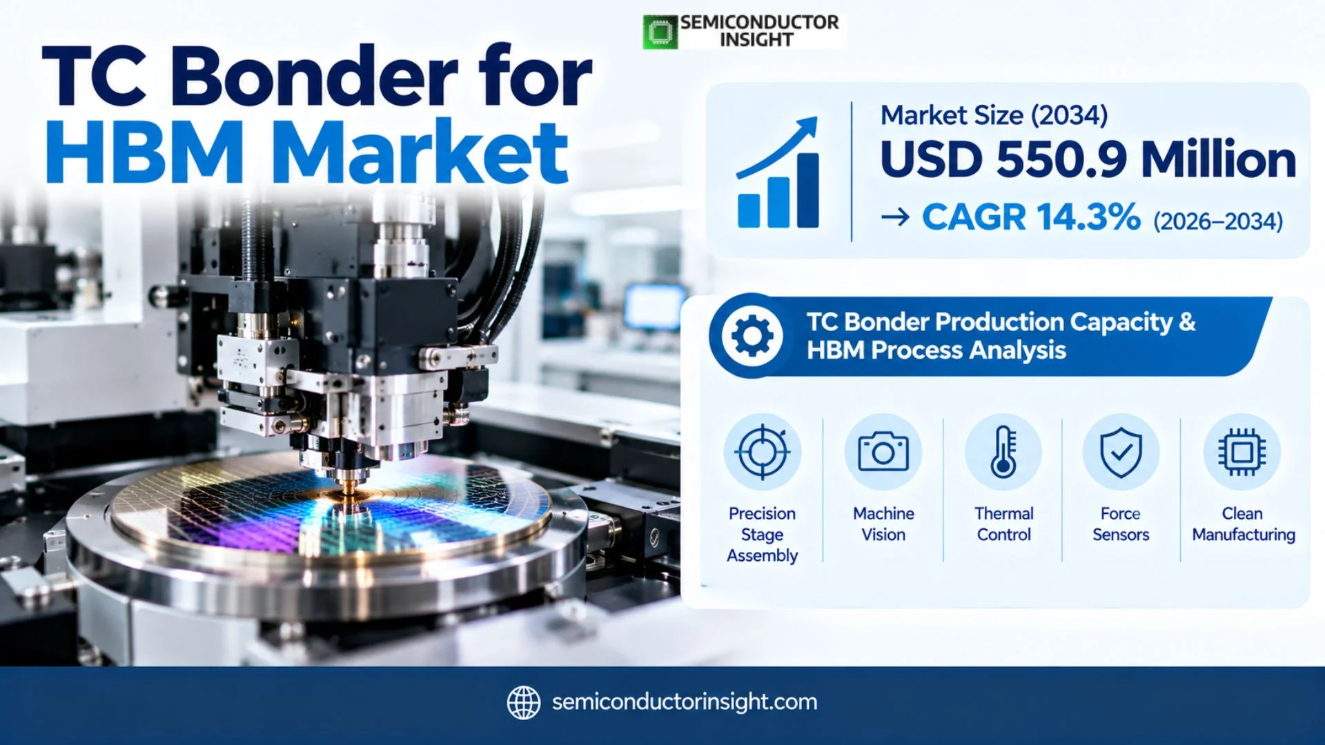
TC Bonder for HBM market is valued at USD 166.0 million in 2025 and is projected to reach USD 550.9 million by 2034, representing a 14.3% CAGR during 2026–2034. The 2026 estimated market size is USD 189.7 million. Asia Pacific is the dominant regional market because HBM memory manufacturing and advanced packaging capacity are concentrated in South Korea, Taiwan and Japan.
Thermocompression bonders are advanced packaging systems that align thin semiconductor dies, apply controlled force and temperature, and create fine-pitch interconnects between vertically stacked memory layers. In HBM manufacturing, bonding accuracy affects interconnect yield, die warpage, underfill behavior, thermal resistance and final stack height. The equipment therefore sits at the intersection of precision motion control, thermal engineering, machine vision and packaging materials.
HBM technology is increasing the difficulty of the bonding step. HBM3E and HBM4 use more layers, thinner dies, tighter bump pitch and higher thermal density than earlier generations. A bonder must maintain sub-micron or micron-class alignment while controlling local force and temperature across warped, ultra-thin dies. Throughput is equally important because even excellent accuracy is not commercially useful if cycle time cannot support memory-volume production.
Two major packaging directions are developing in parallel. TC-MUF and TC-NCF use thermocompression around microbump interconnects with molded underfill or non-conductive film, while hybrid bonding moves toward direct copper-to-copper interconnect with dielectric bonding. Equipment vendors are therefore designing platforms that can improve conventional TCB while preparing customers for smaller pitch and hybrid architectures.
Segment Analysis: By Type
By type, the market is segmented into TC-MUF and TC-NCF. TC-MUF is the leading segment because molded-underfill structures provide strong thermal and mechanical support and are well established in high-density HBM manufacturing.
| Type | Process characteristics | Market position |
|---|---|---|
| TC-MUF | Thermocompression bonding is combined with molded underfill that fills gaps around microbumps and stacked dies. The underfill supports mechanical integrity and thermal cycling while enabling high-volume stack formation. | Leading type. Strong production maturity and thermal/mechanical performance make TC-MUF important for current HBM generations and high-layer stacks. |
| TC-NCF | Non-conductive film is pre-applied or integrated before thermocompression. The film provides insulation and gap fill during bonding and can simplify selected package flows. | A significant alternative where film handling, residue control and bond uniformity fit the customer’s process. It remains important in advanced packaging and selected memory-stack architectures. |
Technology-focus and equipment-capability segmentation
The market is also segmented by technology focus and equipment capability. Conventional TCB remains the largest installed base, while fluxless TCB and hybrid bonding are gaining strategic importance. High-precision alignment is the most critical equipment capability for next-generation HBM, followed by throughput optimization, thermal uniformity and multi-station architecture.
| Axis | Segments | Commercial implication |
|---|---|---|
| By Technology Focus | Conventional TCB · Fluxless / Active-Oxide-Removal TCB · Hybrid Bonding · Advanced Thermal Control | Conventional TCB dominates current production; fluxless processes reduce residue and cleaning; hybrid bonding supports finer interconnect pitch for future HBM and chiplet integration. |
| By Equipment Capability | High-Precision Alignment · Throughput-Optimized · Multi-Station · Warpage / Force Control | Advanced HBM requires accurate vision alignment, controlled force, die-warpage compensation and production throughput without damaging ultra-thin DRAM dies. |
Segment Analysis: By Application
By application, HBM3/3E is the current revenue-leading segment, followed by earlier HBM generations, HBM4 and other advanced memory or heterogeneous-integration applications. HBM4 is the strongest forward equipment-upgrade opportunity because tighter interconnect pitch and more complex stacking push process-control requirements upward.
| Application | Key market insight |
|---|---|
| HBM3 / HBM3E | The current revenue-leading application. AI accelerators and high-performance computing systems use HBM3/3E widely, supporting strong demand for high-throughput TCB systems with reliable thermal and alignment control. |
| HBM4 | Next-generation stacks increase bandwidth and package density and drive tighter pitch, thinner dies and more challenging thermal behavior. Equipment must support stronger alignment, force uniformity and emerging hybrid-bonding paths. |
| Below HBM2E | Earlier HBM and lower-complexity stacks use more mature bonding processes. Demand continues in legacy or cost-sensitive applications but equipment value is lower than advanced HBM generations. |
| AI Accelerator / Chiplet Integration | The same precision-bonding platforms can be adapted to chiplets, logic-memory integration and 2.5D/3D packaging where fine-pitch die-to-wafer placement is required. |
| Other Advanced Packaging | Photonics, co-packaged optics and heterogeneous integration create adjacent opportunities for high-accuracy bonding platforms, especially as hybrid bonding expands. |
Regional Analysis
Asia Pacific dominates the TC Bonder for HBM market, with South Korea, Taiwan and Japan forming the core manufacturing cluster. South Korea is home to major memory suppliers and domestic bonding-equipment companies, Taiwan combines advanced packaging, foundry and OSAT infrastructure, and Japan contributes precision equipment and materials expertise. North America leads important R&D and AI-system demand, while Europe participates in hybrid bonding and advanced packaging equipment.
Why is Asia Pacific central to HBM bonding equipment?
HBM bonding is most valuable when equipment suppliers can work directly with memory manufacturers and advanced-packaging lines. Asia Pacific provides that proximity, allowing rapid process iteration, die-stack experiments, yield learning and equipment customization. North America and Europe remain strategically important through equipment technology, chip design, packaging R&D and future domestic manufacturing.
| Region | Market position | Growth outlook | Core demand | Commercial priority |
|---|---|---|---|---|
| Asia Pacific | Dominant | Very high | HBM memory & advanced packaging | Yield, alignment, throughput and local support |
| North America | R&D / AI demand hub | High | AI, chiplets & advanced packaging | Flexible platforms and next-gen process development |
| Europe | Equipment / hybrid-bonding hub | High | Hybrid bonding, automotive & photonics | Precision, contamination control and efficiency |
| South America | Minimal direct market | Selective | R&D / downstream demand | Installed packaging base |
| Middle East & Africa | Emerging | Selective | Future semiconductor projects | Local packaging infrastructure |
Competitive Landscape
Key participants include HANMI Semiconductor, ASMPT, SEMES, Hanwha Semitech, Yamaha Robotics / SHINKAWA, Besi, Kulicke & Soffa, Toray Engineering, Palomar Technologies, Shinkawa, Shibaura Mechatronics, EV Group, Tokyo Electron, Dai Nippon Printing and Applied Materials. The top five suppliers account for 65% of global revenue, reflecting high technical barriers and close customer qualification.
HANMI Semiconductor is a major HBM thermocompression-bonder supplier with strong positioning in Korean memory packaging. Local proximity to leading DRAM customers supports process co-development, fast service and equipment customization as HBM stack height and pitch evolve.
ASMPT is advancing thermocompression with Active Oxide Removal. Its AOR TCB technology uses a fluxless process to remove oxide during bonding, reducing residue and cleaning requirements while targeting finer pitch, higher-density HBM and chiplet applications. FIREBIRD platforms provide a path from R&D into production.
Besi is strongest in hybrid bonding and advanced assembly. The company reported sharply higher 2026 orders and raised long-term targets as datacenter, photonics and hybrid-bonding demand improved. SEMES, Hanwha Semitech, Yamaha/Shinkawa and Japanese precision-equipment companies broaden competition in conventional TCB and next-generation bonding.
Competitive tier structure
| Competitive tier | Representative companies | Competitive strengths |
|---|---|---|
| HBM TCB leaders | HANMI Semiconductor; ASMPT; SEMES; Hanwha Semitech | HBM process know-how, TC-MUF/TC-NCF, throughput, alignment and memory-customer relationships |
| Hybrid / advanced bonding leaders | Besi; EV Group; Applied Materials; ASMPT | Hybrid bonding, die-to-wafer, fine-pitch interconnect and heterogeneous integration |
| Precision / specialty equipment suppliers | Yamaha/Shinkawa; Toray Engineering; Shibaura Mechatronics; K&S; Palomar; TEL | Precision motion, thermal control, packaging equipment and process-specific bonding |
Key companies profiled
TC Bonder Production Capacity & HBM Process Analysis
Equipment capacity depends on precision-stage assembly, machine vision, bond-head manufacture, thermal-control hardware, force sensors, clean manufacturing and final calibration. Customer output capacity then depends on units per hour, uptime, die-handling yield, recipe changeover and the number of bonders installed on each HBM line.
Throughput is a central commercial variable. HBM contains multiple DRAM layers, so every memory stack requires repeated alignment and bonding operations. Small improvements in seconds per die can materially increase annual output across a large installed tool fleet.
Future HBM4 and hybrid bonding increase the metrology burden. Fine-pitch interconnects tolerate less alignment error, while thinner dies and larger package structures create warpage. Equipment suppliers need better vision, real-time force sensing, temperature uniformity and closed-loop process control.
Market Dynamics
Growth is driven by AI accelerator demand, HBM3E/HBM4 capacity, higher stack counts and advanced packaging. Restraints include equipment cost, precision-component supply, long qualification and technology transition risk. Opportunities center on fluxless TCB, hybrid bonding, multi-station throughput and AI-assisted process control.
MARKET DRIVERS
AI accelerators consume more HBM
Training and inference processors require extremely high memory bandwidth. HBM capacity expansion directly translates into new bonding equipment and higher utilization.
HBM4 tightens process requirements
Finer pitch and higher bandwidth increase alignment and thermal-control requirements, supporting a new upgrade cycle rather than simple reuse of older bonders.
More layers mean more bonding operations
Higher stack counts increase the number of bond steps per finished memory package, magnifying the value of throughput and yield.
Advanced packaging broadens tool utilization
TCB platforms can serve chiplets, logic-memory integration and photonics in addition to HBM, expanding the addressable equipment base.
Drivers Impact Analysis
| Driver | Impact | Primary markets | Time horizon |
|---|---|---|---|
| AI / HPC HBM demand | High | Asia Pacific, North America | Short to long term |
| HBM4 equipment upgrades | High | Korea, Taiwan, Japan | Medium term |
| Higher stack count | High | Memory manufacturers | Persistent |
| Advanced packaging / chiplets | Medium to high | Global | Long term |
MARKET RESTRAINTS
TC bonders are high-capital tools
High-accuracy stages, thermal control and vision systems keep unit prices high, concentrating demand among large memory and packaging companies.
Critical subsystems have concentrated supply
Precision optics, stages, heaters and sensors can create long lead times when advanced-packaging demand accelerates.
Each HBM generation requires qualification
Bond parameters interact with die thickness, bump geometry, underfill and package warpage. Customer approval therefore takes time.
Hybrid bonding can change the equipment mix
Direct copper bonding reduces dependence on conventional bump structures and may shift value toward new tool architectures over time.
Restraints Impact Analysis
| Restraint | Impact | Exposure | Time horizon |
|---|---|---|---|
| High equipment cost | High | Memory / OSAT customers | Persistent |
| Precision-component supply | Medium to high | Equipment OEMs | Short to medium term |
| Qualification time | High | New HBM generations | Persistent |
| Hybrid-bonding transition risk | Medium | Long-term TCB demand | Medium to long term |
MARKET OPPORTUNITIES
Scale fluxless thermocompression
AOR and similar technologies can eliminate flux residue, reduce cleaning and support tighter pitch, improving yield and cost per bit.
Develop HBM4 hybrid-bonding platforms
Future memory stacks may use more direct bonding, creating opportunities for suppliers with die-to-wafer alignment and surface-preparation integration.
Increase multi-station throughput
Parallel or multi-head architectures can reduce effective cycle time and improve capital productivity in high-volume memory fabs.
Use closed-loop analytics for yield optimization
Vision, force, temperature and bond-quality data can be used to adjust recipes in real time and shorten process learning.
TC Bonder for HBM Value Chain Analysis
Precision motion / thermal subsystems
Bonder equipment integration
HBM packaging process
AI / HPC deployment
Precision subsystems set the process window
Stage accuracy and vision determine alignment, while heater and force uniformity determine interconnect quality across the die.
Equipment software converts hardware into yield
Recipe control, warpage compensation, die handling and diagnostics determine whether a bonder can maintain performance across production lots.
HBM packaging multiplies equipment value
Each finished stack contains multiple bonded dies, so a small improvement in bonding yield or cycle time has a large effect on total cost.
AI demand closes the investment loop
Memory manufacturers invest in new bonders when accelerator customers commit to larger HBM volumes and newer generations.
Recent Developments in the TC Bonder for HBM Market
Besi reports strong hybrid-bonding and datacenter demand
Besi’s second-quarter orders rose sharply year over year, with growth led by hybrid bonding, photonics and datacenter applications, indicating stronger advanced-packaging capital demand.
Besi raises long-term financial targets at Investor Day
The company cited stronger demand for 2.5D AI datacenter, photonics and new hybrid-bonding use cases in logic, memory and co-packaged optics.
ASMPT introduces Active Oxide Removal thermocompression bonding
ASMPT presented AOR TCB as a fluxless bonding method designed to reduce residue, improve bonding uniformity and support finer-pitch HBM and chiplet assembly.
ASMPT showcases FIREBIRD and LITHOBOLT for AI and HBM
At ECTC 2026, ASMPT highlighted thermocompression and die-to-wafer bonding platforms for HBM, chiplets and advanced AI packaging.
SK hynix introduces iHBM thermal solution
SK hynix launched a next-generation HBM package using integrated cooling elements and proven MR-MUF packaging concepts, underscoring the growing thermal complexity around stacked memory.
REPORT SCOPE & SEGMENTATION
| Attribute | Details |
|---|---|
| Study Period | 2021–2034 |
| Base Year | 2025 |
| Estimated Year | 2026 |
| Forecast Period | 2026–2034 |
| Historical Period | 2021–2025 |
| Market Size 2025 | USD 166.0 million |
| Market Size 2034 | USD 550.9 million |
| Growth Rate | 14.3% during 2026–2034 |
| Unit | Value (USD Million) and bonder system shipments |
| By Type | TC-MUF · TC-NCF |
| By Application | Below HBM2E · HBM3 / HBM3E · HBM4 · Others |
| By End User | Memory Manufacturers · Foundries · OSAT Providers |
| By Technology Focus | Conventional TCB · Fluxless / AOR TCB · Hybrid Bonding · Advanced Thermal Control |
| By Equipment Capability | High-Precision Alignment · Throughput-Optimized · Multi-Station · Warpage / Force Control |
| By Region | Each region analysed by bonder type, HBM generation, end user, technology focus, equipment capability and country market North AmericaUnited States, Canada EuropeNetherlands, Germany, France and other European markets Asia PacificSouth Korea, Taiwan, Japan, China and other Asian markets South AmericaBrazil and other South American markets Middle East & AfricaIsrael, Saudi Arabia, UAE and other MEA markets |
| Key Companies Profiled | HANMI Semiconductor · ASMPT · SEMES · Hanwha Semitech Co., Ltd · Yamaha Robotics / SHINKAWA · Besi · Kulicke & Soffa · Toray Engineering · Palomar Technologies · Shinkawa Ltd · Shibaura Mechatronics · EV Group · Tokyo Electron Limited · Dai Nippon Printing · Applied Materials |
| Customization Scope | Free report customization equivalent to up to four analyst working days with purchase. Addition or alteration to country, regional and segment scope. |
Frequently Asked Questions
What is the 2025 size of the TC Bonder for HBM market?
The market is valued at USD 166.0 million in 2025 and is projected to reach USD 550.9 million by 2034. The 2026 estimate is USD 189.7 million and the 2026–2034 CAGR is 14.3%.
Which bonder type leads the market?
TC-MUF is the leading type because molded-underfill HBM stacks combine strong mechanical integrity, thermal performance and established production maturity.
Which HBM generation is the largest application?
HBM3 and HBM3E are the current revenue-leading applications, while HBM4 is the major next equipment-upgrade opportunity.
Which region leads the market?
Asia Pacific dominates because South Korea, Taiwan and Japan contain major memory, advanced-packaging and precision-equipment ecosystems.
What is the estimated market size in 2026?
The 2026 estimated market size is USD 189.7 million, consistent with the 2025 and 2032 global market-size endpoints.
Why is bonding precision important in HBM?
Thin DRAM dies and fine microbumps require precise alignment, force and temperature. Small errors can create open connections, warpage, voids or yield loss across the stack.
What are the main market restraints?
High tool cost, precision-component supply constraints, long customer qualification and uncertainty around the transition toward hybrid bonding are the main constraints.
How does HBM4 affect equipment demand?
HBM4 increases stack complexity and interconnect density, requiring tighter alignment, better warpage compensation, stronger thermal control and new hybrid-bonding capabilities.
Which companies are active in the market?
Major participants include HANMI Semiconductor, ASMPT, SEMES, Hanwha Semitech, Yamaha/Shinkawa, Besi, Kulicke & Soffa, Toray Engineering, EV Group and Applied Materials.
What does the report cover?
The report covers TC-MUF and TC-NCF bonders, HBM generations, memory/foundry/OSAT end users, technology focus, equipment capability, five global regions, capacity, dynamics, developments and value chain.
Research Sources & Evidence Base
View primary and authoritative evidence used in this overview
- ASMPT. Thermocompression Bonding with Active Oxide Removal – May 2026 primary evidence on fluxless AOR TCB for HBM and fine-pitch packaging.
- ASMPT. Advanced Bonding for HBM and Chiplets at ECTC 2026 – Official evidence on FIREBIRD thermocompression and LITHOBOLT die-to-wafer bonding platforms.
- Besi. 2026 Investor Day – Primary evidence on stronger hybrid-bonding demand in logic, memory, datacenter and photonics.
- Besi. Q2 2026 Results – Primary evidence on 2026 revenue, orders and hybrid-bonding / datacenter demand.
- SK hynix. iHBM Thermal Solution – May 2026 evidence on HBM packaging thermal requirements and proven MR-MUF architecture.
- SEMI. 3D & Systems Summit 2026 – Industry evidence on hybrid bonding, chiplets and heterogeneous integration trends.

Get Sample Report PDF for Exclusive Insights
Report Sample Includes
- Table of Contents
- List of Tables & Figures
- Charts, Research Methodology, and more...