
Precision Probing Techniques Transforming Semiconductor Device Characterization 2026
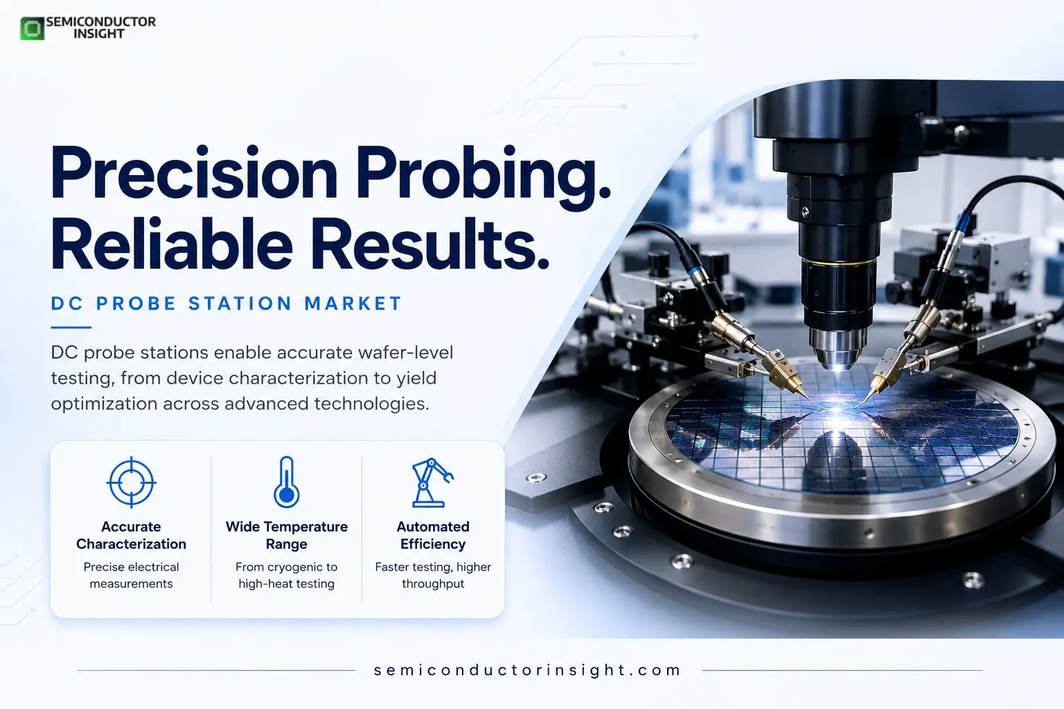
DC probe stations represent specialized platforms designed for precise electrical characterization of semiconductor wafers, dies, and devices at the wafer level. These systems allow engineers to make direct contact with microscopic pads using fine probes, applying controlled voltages and currents while measuring responses in real time. Facilities worldwide, from university cleanrooms to advanced fabrication sites, rely on them for parameter extraction, device modeling, and quality validation before committing resources to full production runs.
The core setup typically includes a stable chuck for holding the wafer, precision manipulators for positioning probes, a high-resolution microscope or camera system for alignment, and integration with source-measure units for accurate data collection. Temperature-controlled chucks expand capabilities to simulate operating conditions ranging from sub-zero cryogenic levels to elevated heat, while shielding options support sensitive low-noise or dark-environment testing.
- Wafer Probing in Semiconductor Research and Development Laboratories
- Academic and corporate R&D centers use DC probe stations to explore new materials and architectures.
- For instance, teams characterizing gallium nitride power integrated circuits have successfully employed DC probes for multi-megahertz crosstalk and substrate coupling measurements, achieving detectable voltage levels as low as single-digit millivolts up to 25 MHz.
- Such work supports development of efficient power electronics for electric vehicles and renewable energy systems.
- Government-backed labs and national nanofabrication networks maintain these tools for open-access research, enabling students and scientists to test novel transistor designs under controlled conditions.
- High Voltage and Thermal Testing Applications in Power Semiconductors
- Power device manufacturers require stations capable of handling thousands of volts safely.
- University projects in regions focused on semiconductor growth have deployed manual systems with thermal chucks reaching 200°C and high-voltage triaxial probe arms up to 3 kV for testing silicon carbide and similar wide-bandgap materials.
- These setups include safety enclosures like laser light curtains to protect operators during high-energy experiments. Real-world examples show successful characterization of MOSFETs and diodes, where precise Kelvin connections minimize measurement errors even at extreme conditions.
-
Automated DC Probing Supporting Advanced Manufacturing Flows
- Fully automated probe stations now integrate wafer loaders, robotic handling, and software for step-and-repeat testing across 200 mm or larger wafers.
- Demonstrations feature systems performing measurements at temperatures from -60°C to 300°C while supporting high-frequency extensions.
- Production environments use them for inline validation, reducing the time from wafer fabrication to actionable electrical data.
- One notable installation allowed full-wafer diagnostics under production conditions, correlating test results seamlessly with existing programs and accelerating yield learning for sub-20 nm nodes.
Curious about the report? Dive into our newest updated version at no cost: https://semiconductorinsight.com/report/dc-probe-station-market/
Cryogenic and Specialized Environment Probing for Cutting-Edge Devices
Research into quantum and low-temperature electronics benefits from cryogenic probe stations that maintain sample integrity below 20 K. Designs place moving components outside the cold zone for reliability, supporting automated testing on up to 100 mm wafers despite vibration from cooling systems.
These platforms deliver repeatable S-parameter and noise measurements critical for radio astronomy amplifiers and superconducting circuits. Dark-box configurations further extend utility to light-sensitive optoelectronic components and sensors.
Integration with Parameter Analyzers for Comprehensive Device Insights
Modern stations pair with multi-channel analyzers offering high-resolution source-measure units, capacitance measurement modules, and waveform generators. This combination enables current-voltage sweeps, capacitance-voltage profiling, and pulsed testing in a single workflow.
Facilities report efficient data collection for process monitoring, with systems handling everything from basic DC parametric checks to complex reliability stress tests. Software suites automate alignment, mapping, and data logging, freeing engineers to focus on interpretation rather than manual operation.
Probe Technology Innovations Enhancing Contact Reliability
Recent advancements include coaxial guarded true-Kelvin MEMS probes with replaceable tips, addressing challenges from shrinking pad sizes and copper metallization.
These designs maintain low and stable contact resistance across thousands of touch-downs, supporting consistent modeling data even on advanced nodes. Such improvements prove vital as devices incorporate finer geometries and heterogeneous integration, where measurement uncertainty can derail development timelines.
Role in Yield Optimization and Early Defect Detection
- By enabling wafer-level electrical fault isolation before dicing, DC probe stations help manufacturers catch issues early in the process.
- Optical and parametric techniques integrated into probing workflows accelerate localization of defects, supporting faster feedback loops between design and fabrication.
- This capability becomes increasingly important with complex 3D stacking and advanced packaging, where traditional post-packaging tests prove insufficient for rapid iteration.
The semiconductor industry continues pushing boundaries in AI accelerators, high-performance computing, and power electronics, with DC probe stations serving as indispensable tools for validation at every stage. Their evolution toward greater automation, wider environmental control, and tighter measurement precision ensures they remain central to bringing reliable, high-performing chips from concept to volume production.

Comments (0)