
The Hidden Layer: How the Pellicle Market Enables Defect-Free EUV Exposure?
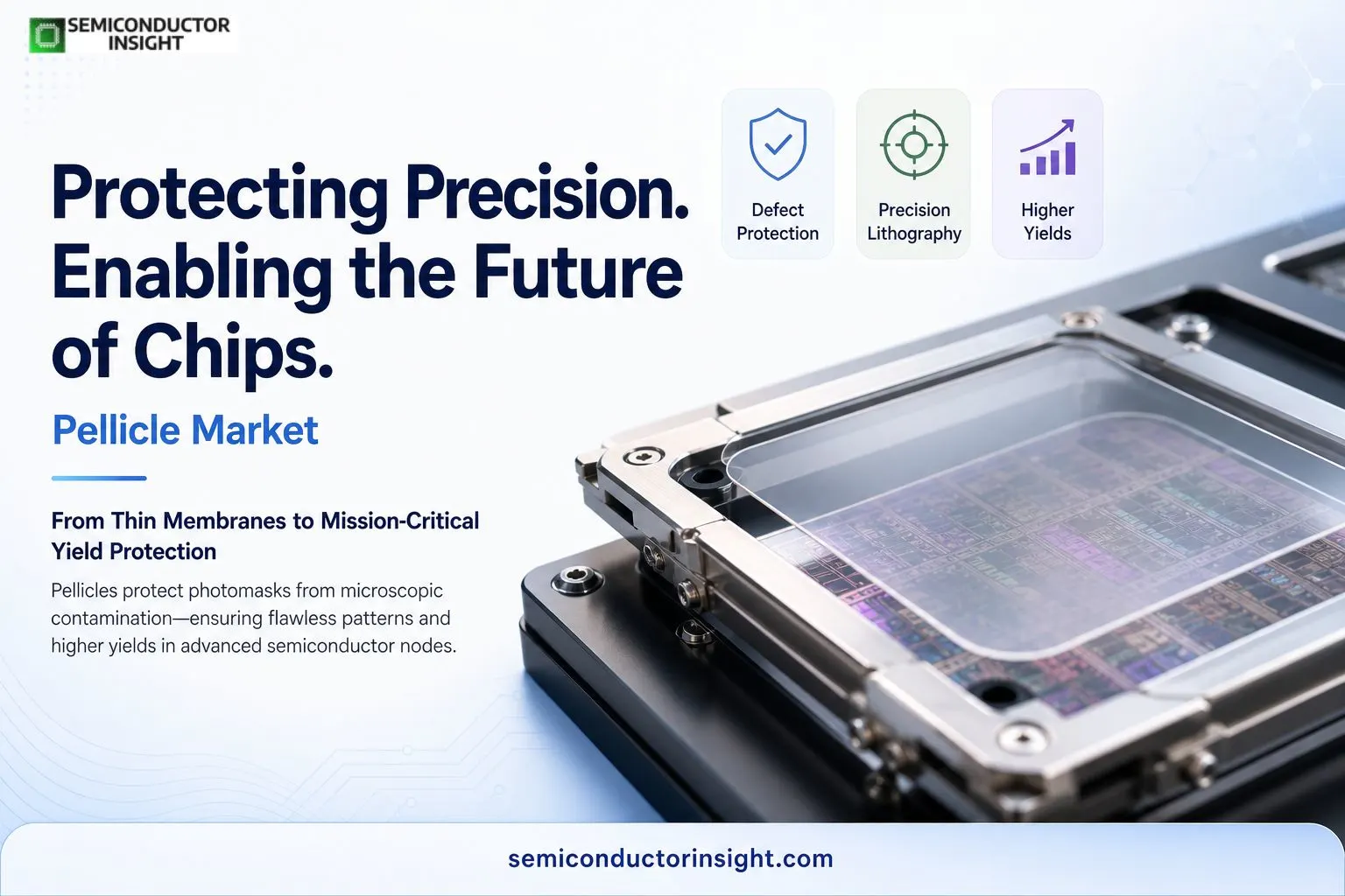
In advanced semiconductor fabrication, even a particle smaller than a micron can destroy a chip worth hundreds of dollars. This is where pellicles quietly play a decisive role. A pellicle is an ultra-thin membrane mounted over a photomask, acting as a barrier that prevents dust or contaminants from landing directly on the mask surface. While this concept dates back to deep ultraviolet lithography, its relevance has surged with the rise of extreme ultraviolet lithography, where defect tolerance is dramatically lower.
At nodes like 5nm and 3nm, manufacturers such as TSMC and Samsung Electronics operate in environments where a single defect can compromise entire wafers. Pellicles ensure that contaminants remain out of focus during exposure, preventing pattern distortion and yield loss.
EUV Lithography Advancing Pellicle Material Boundaries
The shift toward extreme ultraviolet lithography has redefined pellicle development as a highly specialised materials engineering challenge.
Operating at an ultra-short wavelength, EUV systems require pellicles that are exceptionally thin while still delivering high optical transparency and structural stability. In contrast to previous lithography techniques, the exposure environment in EUV provides a high concentration of energy, subjecting pellicle membranes to constant mechanical and thermal stress.
For instance, in February 2026,
- LINTEC has created a novel coating composition that greatly increases the longevity of carbon nanotube (CNT) pellicles used in Extreme Ultraviolet (EUV) lithography.
- By collaborating with the Semiconductor Frontier Research Centre of the National Institute of Advanced Industrial Science and Technology (AIST) on mass-production technologies, LINTEC is advancing research and development with the goal of creating a first mass-production system for CNT pellicles, which are clean-conservation materials necessary for creating fine patterns in advanced semiconductors.
This has forced a transition away from conventional polymer-based films toward more advanced material solutions. Engineers are now focusing on silicon-based membranes and emerging nanostructured materials that can maintain optical clarity while resisting deformation under prolonged exposure. The emphasis is no longer just on protection from contaminants but on ensuring uninterrupted performance in increasingly demanding fabrication conditions.
High NA EUV Opening New Directions in Pellicle Innovation
The emergence of High Numerical Aperture EUV systems is adding another layer of complexity to pellicle design. These systems enhance resolution capabilities but also intensify the energy density directed at the pellicle surface, amplifying thermal and mechanical strain. To address this, researchers and manufacturers are exploring ultra-thin film technologies that balance durability with minimal interference in the lithography process.
Materials such as silicon nitride and graphene are gaining attention for their ability to combine strength, flexibility, and efficient heat dissipation. These next-generation materials are being studied not only for their resilience but also for their ability to support the precision required in advanced semiconductor patterning. As lithography tools continue to evolve, pellicle innovation is moving in parallel, driven by the need to sustain both performance and reliability in next-generation chip manufacturing environments.
Go through the most recent report update to learn more before proceeding: https://semiconductorinsight.com/report/global-pellicle-market-trends-business-strategies-2025-2032/
High Impact Pellicle Linkage and Risk Mapping
- Pellicle importance rises sharply as semiconductor nodes shrink, with each advanced node depending on a more specialised protection layer to preserve mask integrity and production yield.
- At the 28 nm node, KrF pellicles used with 248 nm lasers carry a relatively low risk, while the 7 nm node relies on ArF pellicles with 193 nm immersion technology, where the risk level becomes moderate.
- As the industry moves to 5 nm and 3 nm nodes, EUV Low-NA processes require MoSi or Si pellicles, making the dependence significantly higher.
- At the 2 nm node, EUV 0.33 NA platforms demand high-durability MoSi solutions, pushing the criticality to a very high level. Beyond 1.4 nm, High-NA EUV is expected to require CNT pellicles, which are considered critical for maintaining process stability.
- The cost impact also escalates with each node transition, since pellicle expense becomes a larger part of the total mask value.
- A EUV mask can cost around $300,000, so the failure or absence of a pellicle can lead to mask scrapping and repeated defects across all wafers in the lot.
- This makes pellicle reliability not just a technical requirement, but a direct economic safeguard in advanced chip manufacturing.
The invisible technology powering visible innovation
While pellicles rarely make headlines, their impact is deeply embedded in every advanced chip produced today. From powering AI models to enabling next-generation smartphones, their role is foundational.
As semiconductor nodes continue to shrink and complexity rises, pellicles will evolve from passive protective layers into highly engineered components that directly influence performance, yield, and cost efficiency. The pellicle market is not just growing; it is becoming indispensable to the future of computing.

Comments (0)