
Most Dominating 8 Deposition Techniques Elevating Semiconductor Film Performance Worldwide
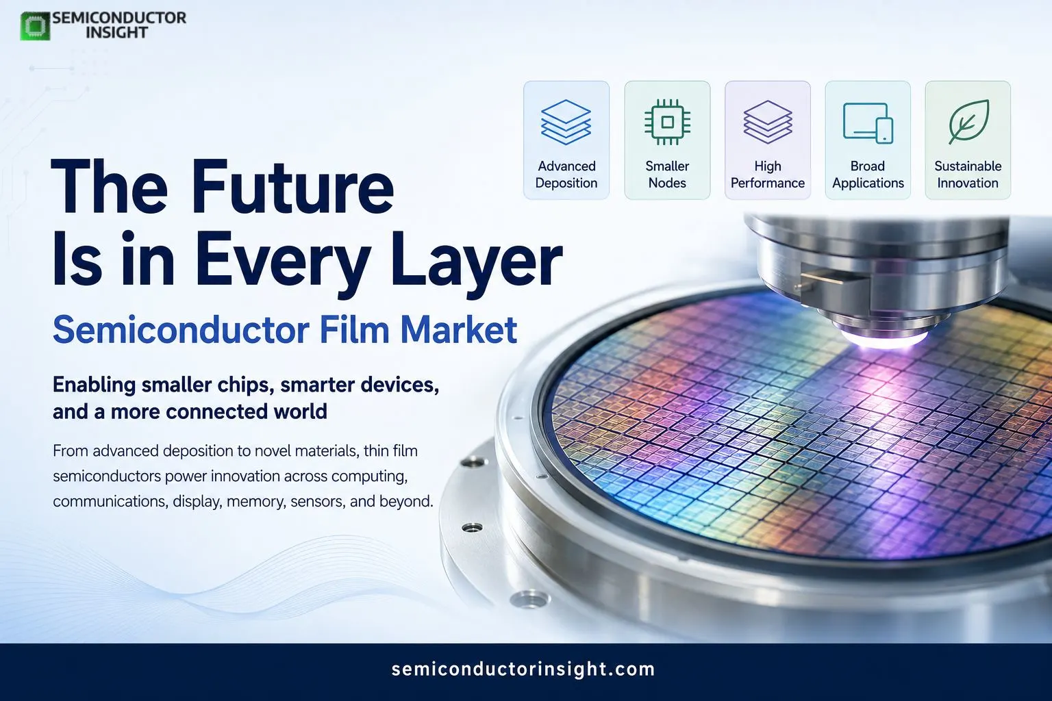
Thin film semiconductors form the invisible backbone of nearly every modern electronic device. These layers, often just a few nanometers thick, are deposited onto silicon wafers or other substrates using techniques like chemical vapor deposition and physical vapor deposition. Their precise control enables the tiny transistors and interconnects that power everything from smartphones to data centers.
In major fabrication facilities, engineers deposit hundreds of thin film layers per wafer during the manufacturing sequence. For advanced nodes, the cumulative volume of materials processed across global foundries supports production of billions of chips annually. Government reports on semiconductor initiatives highlight investments in expanding deposition tool capacities to meet rising demand from artificial intelligence and high-performance computing sectors.
Precision Deposition Driving Smaller Device Architectures
- Atomic layer deposition has gained prominence for its ability to create conformal coatings on complex 3D structures.
- In one documented implementation at a leading logic manufacturer, this method allowed uniform gate dielectrics on fin-shaped transistors, significantly improving electrical performance and reducing leakage.
- Such advancements support the transition to smaller process nodes where traditional methods face physical limits.
- Latest study descriptions of thin film technology detail how these layers enable integrated circuits by providing insulators, conductors, and semiconductors in stacked configurations.
Thin Films in Memory and Storage Technologies
Dynamic random access memory and NAND flash devices rely heavily on thin film capacitors and charge trap layers. Production lines in South Korea and Taiwan have scaled output to handle enormous wafer starts each month, with thin film processes contributing to higher density cells. Ongoing examples include the integration of high-k dielectric films that store more charge in smaller areas, directly impacting storage capacities in consumer and enterprise drives.
Optoelectronics and Display Applications
Semiconductor films play a starring role in light emitting diodes and advanced display panels. Organic and inorganic thin films enable vibrant colors and flexibility in next generation screens used in foldable devices and large format televisions. Manufacturers report enhanced efficiency through optimized deposition of active layers, leading to brighter outputs with lower power consumption in real deployed products.
Before Proceeding, Feel Free to Overlook Our Updated Report: https://semiconductorinsight.com/report/semiconductor-film-market/
Sensor Technologies Benefiting From Specialized Films
Thin film semiconductors appear in a growing array of sensors for automotive safety, environmental monitoring, and medical diagnostics. Case studies from research institutions show how deposition on flexible substrates creates wearable health monitors capable of detecting subtle biometric signals. These films offer sensitivity and response times that rigid silicon alternatives struggle to match in certain environments.
Plasma Enhanced Processes Enhancing Film Quality
- Plasma enhanced chemical vapor deposition allows lower temperature processing, which protects delicate structures in back end of line fabrication.
- Industrial articles describe its use in depositing dielectric layers that insulate interconnects, reducing crosstalk in high speed chips.
- Facilities have adopted these methods to maintain throughput while achieving the defect densities required for yields above 90 percent on large wafers.
Material Innovations Supporting Green Manufacturing
Efforts to reduce waste in thin film deposition include recycling precursor gases and optimizing chamber cleaning cycles. Authorized technical resources outline how newer processes minimize hazardous byproducts, aligning with international environmental standards. In practice, several fabs have reported measurable reductions in material usage per wafer through improved uniformity and process control.
Emerging Uses in Power and Specialty Semiconductors
- Wide bandgap materials benefit from thin film techniques for creating efficient power devices used in electric vehicles and renewable energy inverters.
- Real deployments show these films enabling higher switching frequencies and lower losses, which translates to better system efficiency.
- Research publications detail ongoing work on gallium nitride and silicon carbide films deposited via epitaxial methods for superior performance characteristics.
The semiconductor film domain continues to evolve rapidly as device complexity increases. From everyday consumer gadgets to specialized industrial applications, these precisely engineered layers deliver the functionality that defines contemporary technology. Their ongoing refinement ensures the industry can sustain the pace of innovation demanded by global digital transformation.

Comments (0)