
How MOCVD Market Is Changing Due to Compound Semiconductor Growth?
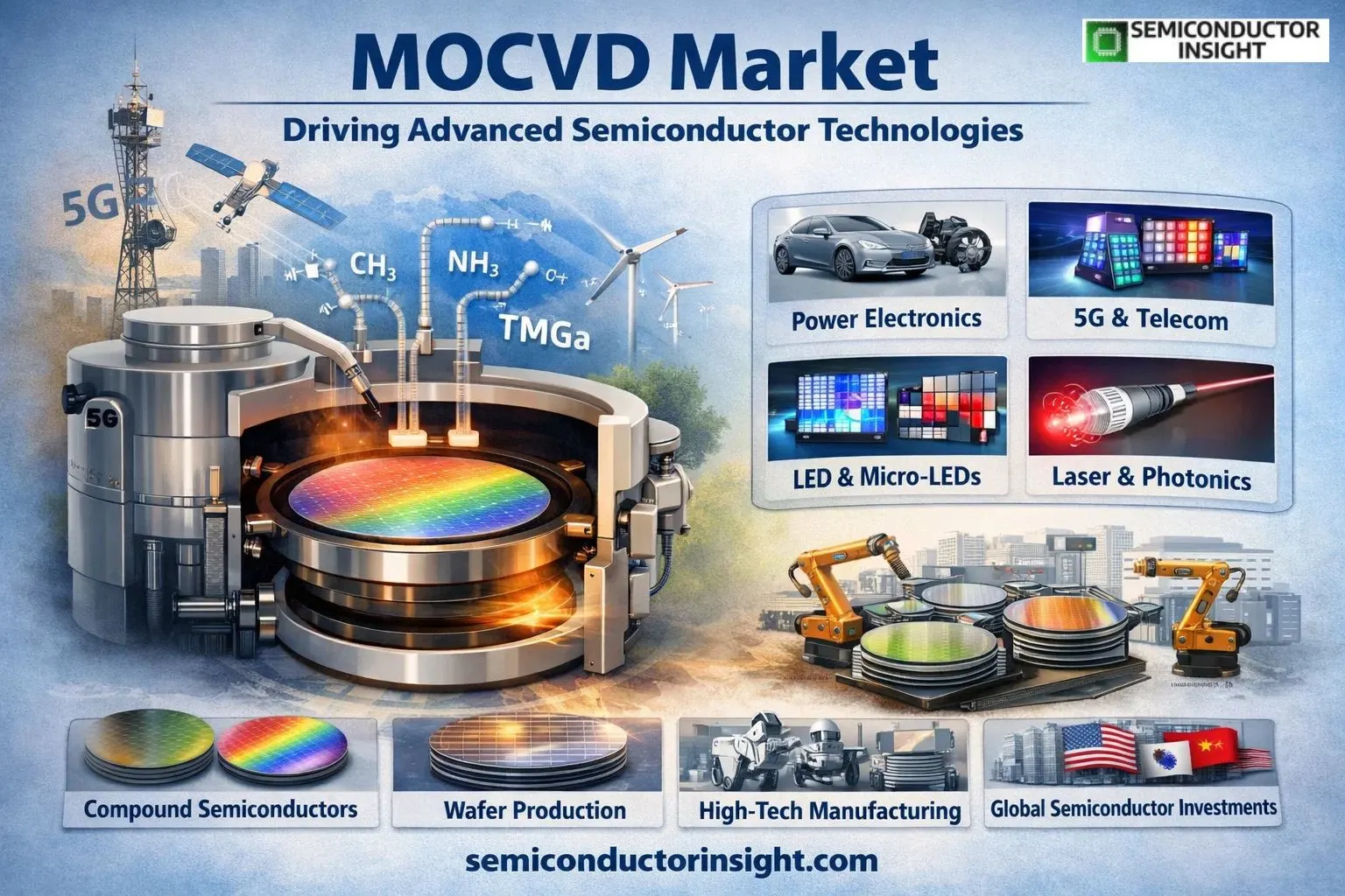
Metal-Organic Chemical Vapor Deposition (MOCVD) has become one of the most important technologies in modern semiconductor fabrication. It is a process used to grow extremely thin crystalline layers on semiconductor wafers through controlled chemical reactions between metal-organic compounds and gases inside high-temperature reactors. These layers form the foundation for advanced electronic and optoelectronic devices. MetalOrganic Chemical Vapor Deposition systems allow engineers to deposit materials with atomic-level precision, which is essential for building high-performance semiconductor structures.
The technology is widely used for producing compound semiconductors such as gallium nitride, gallium arsenide, and indium phosphide. These materials support the development of devices used in telecommunications, lasers, power electronics, and high-frequency integrated circuits.
Today, MOCVD Market is closely linked to the rapid expansion of digital infrastructure, high-speed communications, and energy-efficient electronics.
Advanced Materials Powering the Compound Semiconductor Market
- One of the defining characteristics of MOCVD technology is its ability to grow epitaxial semiconductor layers with extremely high uniformity. During deposition, metal-organic precursor gases react on heated substrates, forming crystalline layers that replicate the atomic structure of the underlying wafer.
- This process enables the fabrication of compound semiconductor materials such as gallium nitride (GaN) and gallium arsenide (GaAs). These materials offer superior electron mobility and thermal stability compared with conventional silicon. As a result, they are widely used in radio-frequency amplifiers, laser diodes, and high-efficiency power devices.
- For instance, gallium nitride wafers account for nearly 38% of compound semiconductor wafer production used in power electronics and high-frequency applications.
- Such materials are especially important for applications requiring high power density, including electric vehicle power modules and satellite communication systems.
Role in LED and Display Manufacturing
One of the largest industrial applications of MOCVD technology is the manufacturing of light-emitting diodes. MOCVD reactors are used to grow the semiconductor layers required to produce LED chips for lighting and display technologies.
LED manufacturing alone represents more than 41% of total MOCVD-based semiconductor applications, reflecting the growing demand for energy-efficient lighting and advanced display systems.
Beyond conventional LEDs, emerging display technologies such as micro-LED and mini-LED displays rely heavily on precise epitaxial growth processes. These displays are increasingly used in smartphones, augmented-reality devices, and high-definition televisions.
For example, several display manufacturers are planning to shift nearly 40% of their display production capacity toward micro-LED technologies, which require advanced MOCVD deposition systems.
You Can Go Through Our Latest Updated Insights Here: https://semiconductorinsight.com/report/mocvd-market/
Engineering Performance of Modern MOCVD Reactors
Modern MOCVD reactors are highly sophisticated semiconductor manufacturing tools. These systems operate at extremely controlled temperatures and pressures to ensure consistent crystal growth.
Advanced reactors can maintain temperature precision of around ±0.5 °C and thin-film thickness uniformity within ±1%, allowing semiconductor manufacturers to produce highly consistent wafers.
Many production systems also support batch processing of more than 60 wafers in a single growth cycle, significantly improving manufacturing throughput for semiconductor fabrication plants.
Automation and in-situ monitoring technologies are increasingly integrated into these reactors. Recent installations show that nearly 48% of advanced MOCVD tools now include real-time monitoring systems that help control defect density and optimize layer thickness during production.
Industry Applications across Multiple Technology Sectors
MOCVD technology plays a crucial role across multiple semiconductor industries. Its ability to produce high-quality compound semiconductor layers makes it essential for several emerging technologies.
- High-frequency RF devices used in 5G communication infrastructure
- Power electronics for electric vehicles and renewable energy systems
- Laser diodes and photonic devices used in optical communication
- Advanced sensors used in aerospace and defence technologies
- Micro-LED displays used in smartphones and wearable electronics
Semiconductor manufacturing accounts for nearly 66% of total MOCVD technology usage, highlighting its importance in the global electronics industry.
Government Semiconductor Programs and Strategic Investments
Several countries are increasing investments in semiconductor manufacturing infrastructure, which indirectly supports the expansion of the MOCVD Market. Government initiatives focused on semiconductor independence are funding new fabrication plants dedicated to compound semiconductor production.
For example, national semiconductor programs in the United States and Asia have allocated hundreds of millions of dollars for advanced semiconductor equipment development and domestic fabrication capacity expansion. These programs aim to strengthen supply chains for strategic technologies such as 5G communications, defense electronics, and electric vehicles.
In many cases, these investments focus specifically on compound semiconductor technologies because of their importance in next-generation electronic systems.
The Expanding Importance of Precision Thin-Film Engineering
The increasing complexity of semiconductor devices requires highly controlled fabrication techniques. MOCVD technology provides the precision needed to build multi-layer semiconductor structures used in modern electronics.
With continued growth in telecommunications, renewable energy systems, and advanced computing technologies, the importance of epitaxial growth and compound semiconductor materials continues to increase.
As a result, MOCVD Market is expected to remain closely tied to innovations in semiconductor materials science, enabling new generations of high-performance electronic and photonic devices.

Comments (0)