
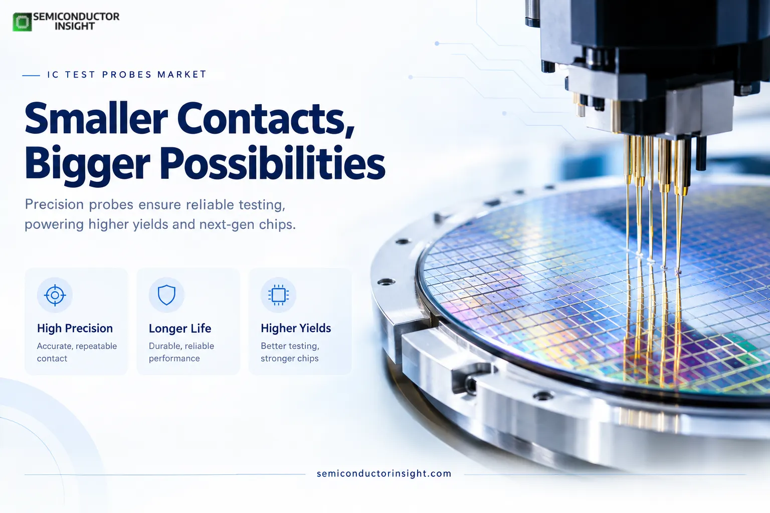
MEMS vs. Traditional IC Test Probes in 2026 Which Contact Architecture Fits Advanced Chips
The semiconductor industry’s most visible innovations happen inside processors, memory devices and advanced packages. Yet before those chips reach a system, another highly specialized technology has to establish whether individual dies actually work. IC test probes perform that deceptively simple job by creating temporary electrical contact between test equipment and semiconductor devices during wafer-level testing.
As chip geometries become smaller and architectures become more complicated, the probe is no longer just a mechanical contact. It has become a precision-engineered interface where electrical performance, contact force, pitch, durability, thermal behavior and signal integrity all have to work together.
The Contact Point Is Getting Smaller
Modern wafer testing is being pushed toward increasingly fine contact geometries. FormFactor, for example, describes its Takumi parametric probe-card technology as supporting 40 µm pad pitch, while its MEMS MicroSpring contact architecture is designed for more than 1 million touchdowns.
That scale matters because smaller contact pads allow manufacturers to increase die density and make more efficient use of wafer real estate. The probe therefore has to land accurately without damaging the pad or introducing unstable electrical resistance.
The basic progression can be represented as:
Smaller device geometry → Smaller test pads → Tighter probe placement → Higher contact precision → Reliable wafer-level measurement
A Probe Is Now Part of the Yield Equation
- The economic importance of probing comes from its position in the manufacturing sequence.
- A wafer may contain hundreds or thousands of individual dies, and wafer sort identifies defective devices before they move into more expensive packaging and final-test stages.
- Probe cards therefore have to deliver repeatable electrical contact across large numbers of touchdowns.
- Even a small contact-resistance variation can affect measurement consistency, particularly when manufacturers are testing increasingly sensitive semiconductor structures.
- FormFactor notes that advanced wafer testing requires tighter control of pad pitch, probe force, contact resistance and parallelism as semiconductor technologies continue scaling.
AI and HBM Are Changing What “Good Contact” Means
The rapid expansion of AI processors and high-bandwidth memory is creating a particularly demanding testing environment. SEMI reported that global semiconductor test-equipment billings increased 55% in 2025, with AI devices and HBM cited among the factors increasing performance requirements and test intensity.
HBM introduces additional complexity because multiple memory dies are ultimately integrated into a high-density stack. Teradyne’s HBM test platform, for example, supports testing from base-die wafer test through memory-core testing and burn-in, including HBM2E, HBM3, HBM3E, HBM4 and HBM4E.
For probe technology, this creates demand for interfaces capable of handling increasingly dense electrical connections while maintaining repeatability.
The Numbers behind the New Testing Environment
The semiconductor industry’s manufacturing scale provides another indication of why probe technology matters. Worldwide silicon-wafer shipments reached 12,973 million square inches in 2025, according to SEMI, while demand for 300 mm wafers remained particularly strong in AI-related logic and HBM applications.
At the same time, SEMI reported 18 new fab construction projects beginning in 2025, including 15 300 mm facilities and three 200 mm facilities.
More wafers, more advanced devices and more complex packages ultimately translate into more opportunities for wafer-level inspection and electrical testing.
MEMS Is Changing the Physical Design of the Probe
- One of the most interesting developments is the increasing use of MEMS-based contact structures. Instead of relying only on conventional mechanical needle arrangements, MEMS architectures can create highly controlled three-dimensional contact structures.
- The advantage becomes particularly relevant when the test interface must combine fine pitch, low contact resistance, mechanical compliance and long operating life.
- This is also where durability becomes a measurable engineering parameter. FormFactor’s Takumi technology specifies a greater-than-1-million-touchdown lifetime for its 3D MEMS MicroSpring contact.
Our most recent updated related study is available for free at this link: https://semiconductorinsight.com/report/ic-test-probes-market/
Cleaning Is Becoming an AI Problem
Probe contamination is another area undergoing a technological shift. Semiconductor manufacturers traditionally cleaned probe needles at predetermined intervals. Advantest has introduced an Adaptive Probe Cleaning approach that uses AI algorithms to determine when probe cleaning is actually required rather than relying solely on fixed cycles.
The significance is subtle but important. Excessive cleaning can consume production time and shorten probe-card life, while insufficient cleaning can reduce test yield. AI-based monitoring attempts to find the point between those two outcomes.
Fixed cleaning schedule → Probe-condition monitoring → AI assessment → Cleaning only when required → Higher availability
Chiplets Are Creating More Places to Test
Advanced packaging is also altering the probing landscape. Semiconductor designs increasingly combine multiple dies or chiplets within one package, creating additional interfaces that must be characterized and validated.
SEMI notes that chiplet-based advanced packaging is creating an explosion of test insertion points, increasing both test complexity and the sophistication required from test and assembly operations.
This is pushing probe technology beyond traditional wafer-sort requirements toward interfaces capable of supporting heterogeneous architectures and increasingly complicated test flows.
The Probe Card Is Becoming a Data Interface
The next evolution is not simply about making probes smaller. It is about connecting the physical contact layer with increasingly intelligent testing systems.
Recent developments illustrate this direction. In July 2026, Advantest expanded its SiConic ecosystem into Design-for-Test engineering, specifically addressing advanced-node SoCs, AI accelerators and chiplet-based architectures where larger pattern volumes and sophisticated DFT methodologies are becoming necessary.
The result is a new testing chain:
Device design → DFT architecture → Probe interface → Automated measurement → Yield data → Process feedback
That connection turns IC test probes into more than passive hardware. They become one of the physical links between semiconductor design intelligence and manufacturing intelligence.
Where the Market Is Becoming Most Specialized
- The strongest technical differentiation is emerging around a handful of requirements rather than a single universal probe design.
- Fine-pitch logic devices demand contact precision; HBM requires dense and reliable interfaces; power semiconductors introduce different electrical and thermal requirements; while chiplets increase the number and complexity of test insertion points.
- For probe manufacturers, the opportunity is therefore moving toward application-specific contact architectures rather than one-size-fits-all interfaces.
The Smallest Hardware Is Solving Some of the Biggest Chip Problems
The IC test probes market sits in an unusual position within semiconductor manufacturing. It does not manufacture the processor, memory cell or package itself, but it determines whether those structures can be accurately measured before moving further through the production chain.
As semiconductor manufacturing moves toward sub-3 nm logic, HBM4-class memory, AI accelerators, chiplets and increasingly dense packaging, the humble electrical contact is becoming a high-precision technology platform. The next generation of IC testing will depend not merely on touching more devices, but on making every contact smaller, cleaner, faster, more repeatable and increasingly intelligent.

Comments (0)