MEMS Probe Card vs. Vertical Probe Card Market 2026 Which Technology Is Leading Advanced Wafer Testing
Every semiconductor chip undergoes extensive testing before it reaches smartphones, automobiles, AI servers, or industrial equipment. Hidden within this quality assurance process is one of the industry’s most precise tools the probe card. While often overshadowed by lithography systems and advanced packaging technologies, probe cards play an essential role in ensuring that integrated circuits function correctly before moving to subsequent manufacturing stages.
As semiconductor companies accelerate production of artificial intelligence processors, high-bandwidth memory, automotive chips, and advanced logic devices, the Probe Card Market is gaining unprecedented importance within the semiconductor value chain.
Inside the Testing Stage Where Every Contact Point Matters
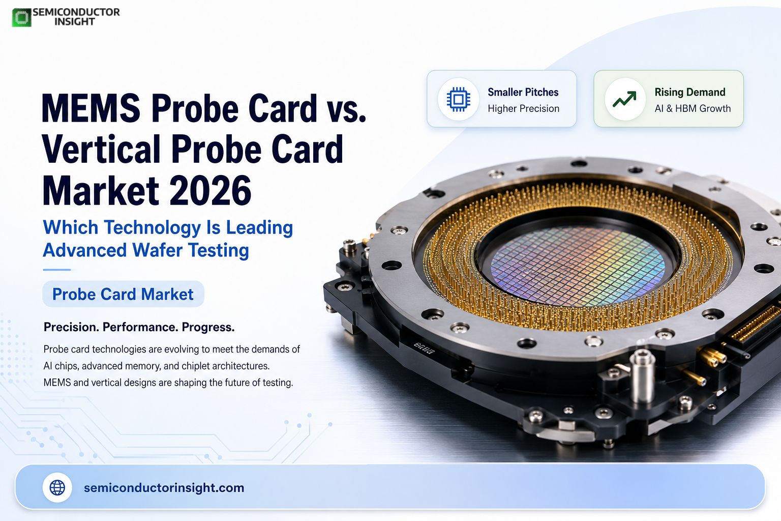
Probe cards act as the physical interface between automated test equipment and semiconductor wafers. Thousands of microscopic probes establish temporary electrical connections with chip pads, allowing engineers to evaluate functionality, performance, and manufacturing quality before chips are packaged.
Semiconductor Testing Journey
Wafer Fabrication
↓
Wafer Inspection
↓
Probe Card Contact Testing
↓
Electrical Validation
↓
Chip Selection
↓
Packaging and Assembly
↓
Final Product Deployment
A single testing session may involve thousands of simultaneous contact points, particularly for advanced processors and memory devices designed for data-intensive applications.
AI Chips Are Creating New Testing Demands
The explosive growth of generative AI infrastructure is increasing complexity throughout semiconductor manufacturing.
Modern AI accelerators contain billions of transistors and significantly larger die sizes than conventional processors. According to publicly available technical disclosures from leading semiconductor manufacturers, advanced AI processors can contain well over 100 billion transistors on a single package.
This complexity directly affects wafer testing requirements.
Why AI Changes Probe Card Requirements?
✓ Higher pin counts
✓ Smaller contact pitches
✓ Increased testing precision
✓ Faster throughput demands
✓ Greater thermal management requirements
Probe card developers are therefore designing solutions capable of handling more sophisticated testing environments than those used only a few years ago.
Semiconductor Scale and Its Impact
The semiconductor industry offers a clear picture of why probe card technology is becoming increasingly important. In 2025, global semiconductor revenue is expected to exceed USD 620 billion, while advanced fabs typically operate on 300 mm wafers and produce logic nodes below 5 nm. High-end AI processors now integrate more than 100 billion transistors, and major fabrication plants process tens of thousands of wafers every day. These figures reflect the scale, precision, and testing demands that continue to drive the need for advanced probe card solutions.
Sources for these figures include annual reports, technical publications, and semiconductor industry organizations such as the Semiconductor Industry Association, along with disclosures from leading chip manufacturers.
The Shift from Simple Needles to Precision Micro Engineering
Traditional Cantilever Probes
↓
Vertical Probe Architectures
↓
MEMS Probe Technology
↓
Ultra Fine Pitch Designs
↓
Advanced AI and HBM Testing Platforms
Modern MEMS-based probe cards provide improved alignment accuracy, durability, and scalability for advanced semiconductor devices. These capabilities are increasingly important for high-performance computing processors and advanced memory products.
Memory Devices Are Quietly Expanding Testing Requirements
While AI processors attract headlines, memory technologies are creating equally important opportunities.
The growing adoption of High Bandwidth Memory (HBM) in AI servers has increased wafer-level testing complexity. Each HBM stack contains multiple memory dies that require rigorous validation before integration into advanced packages.
Recent investments by major memory manufacturers have expanded production capacity for advanced DRAM and HBM products, creating additional demand for high-precision testing solutions.
For More Detailed Insights, You Can Surf Our Latest Report Here: https://semiconductorinsight.com/report/probe-card-market/
Application Focus Map
AI Accelerators → High Density Probe Cards
HBM Memory → Fine Pitch Testing
Automotive Chips → Reliability Validation
Power Devices → Electrical Performance Testing
Chiplets → Advanced Interconnect Verification
Probe Technology Spotlight beyond Traditional Testing Platforms
- As semiconductor geometries continue to shrink, manufacturers are increasingly evaluating MEMS probe cards and vertical probe cards for different testing needs.
- MEMS probe cards stand out for their very high contact density and excellent fine-pitch capability, making them especially suitable for advanced logic and AI processors that require precise signal integrity.
- Vertical probe cards, on the other hand, offer strong mechanical stability and remain a reliable choice for applications such as AI processor testing and advanced memory testing.
- Overall, MEMS-based designs are gaining attention for next-generation devices where extremely small contact pitches and high accuracy are essential.
The Rise of Chiplets Is Changing Testing Strategies
One of the most important developments influencing probe card design is the adoption of chiplet architectures.
Instead of manufacturing a single monolithic processor, companies increasingly combine multiple smaller dies within one package. This approach improves manufacturing flexibility but also introduces additional testing requirements at both wafer and package levels.
As chiplet-based products become more common in data center processors, networking hardware, and AI accelerators, probe card technology continues evolving to support increasingly sophisticated semiconductor ecosystems.
The Probe Card Market therefore occupies a unique position within semiconductor manufacturing. Every advancement in AI computing, memory technology, advanced packaging, and chiplet integration ultimately increases the importance of accurate wafer-level testing making probe cards one of the industry’s most essential yet often overlooked technologies.
Comments (0)