
MARKET INSIGHTS
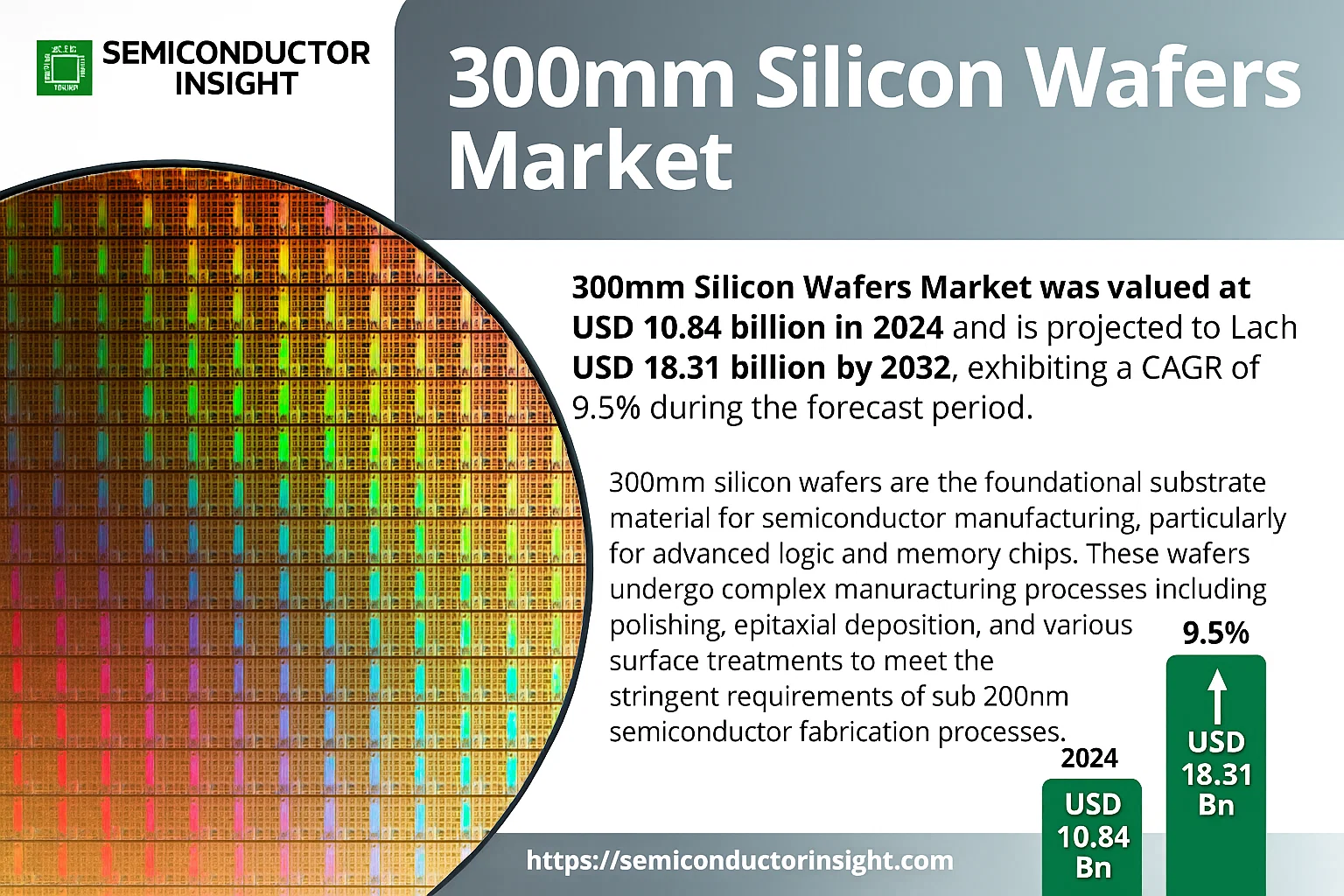
Global 300mm Silicon Wafers Market was valued at USD 10.84 billion in 2024 and is projected to reach USD 18.31 billion by 2032, exhibiting a CAGR of 9.5% during the forecast period.
300mm silicon wafers are the foundational substrate material for semiconductor manufacturing, particularly for advanced logic and memory chips. These wafers undergo complex manufacturing processes including polishing, epitaxial deposition, and various surface treatments to meet the stringent requirements of sub-20nm semiconductor fabrication processes.
The market growth is primarily driven by increasing demand for advanced computing devices, expansion of 5G infrastructure, and the ongoing digital transformation across industries. The semiconductor industry’s shift toward smaller process nodes (below 20nm) has increased the consumption of premium-quality 300mm wafers, as these advanced processes require flawless substrate materials. Additionally, government initiatives to strengthen domestic semiconductor supply chains, particularly in the U.S., Europe, and China, have accelerated investments in wafer manufacturing capacity.
However, the market faces challenges including high capital expenditure requirements (a single 300mm wafer fab costs over $5 billion), complex supply chain dependencies (particularly for semiconductor-grade silicon materials and equipment), and geopolitical tensions affecting the global supply chain. The market is currently dominated by Japanese and Korean manufacturers, though Chinese manufacturers are rapidly expanding their capacity with government support.
According to SEMI’s latest report, global 300mm wafer fab capacity is expected to reach 7.2 million wafers per month (wpm) by 2024, representing a 9% increase from 2023. The foundry segment accounts for approximately 51% of this capacity, followed by memory at 37%. Taiwan remains the largest region for 300mm wafer production, followed by South Korea and China.
MARKET DRIVERS
Exponential Demand for Advanced Logic and Memory Chips
The primary driver for the 300mm silicon wafer market is the insatiable global demand for advanced semiconductor devices. The proliferation of 5G technology, artificial intelligence, high-performance computing, and the Internet of Things (IoT) necessitates chips built on the most advanced process nodes, which are predominantly manufactured on 300mm wafers. This larger wafer size offers superior economies of scale, producing significantly more dies per wafer compared to 200mm wafers, thereby reducing the cost per chip for high-volume production.
Government Investments and Semiconductor Sovereignty
Substantial government initiatives worldwide, such as the CHIPS and Science Act in the United States and the European Chips Act, are injecting billions into domestic semiconductor manufacturing capacity. A significant portion of these investments is directed toward building new state-of-the-art fabs or expanding existing ones that are capable of processing 300mm wafers. This policy-driven push is a powerful force creating a predictable, long-term demand for 300mm silicon wafers.
➤ The transition to smaller process nodes below 10nm is essentially synonymous with 300mm wafer processing, locking in demand from leading-edge foundries.
Furthermore, the continuous miniaturization of semiconductor components drives the need for the superior flatness, purity, and defect control that 300mm wafers provide. As chipmakers push toward 3nm, 2nm, and beyond, the specifications for starting silicon substrates become exponentially stricter, a standard that is most consistently met by the 300mm wafer manufacturing ecosystem.
MARKET CHALLENGES
Extreme Capital Intensity and High Barriers to Entry
The 300mm wafer market is characterized by exceptionally high capital expenditure. Constructing a new 300mm wafer fab can cost upwards of $20 billion. This immense financial barrier limits the number of players who can participate in the leading-edge segment of the market, concentrating power among a few large multinational corporations like TSMC, Samsung, and Intel. The cost of the wafer fabrication equipment (WFE) required for 300mm processing is also substantially higher than for smaller wafer sizes.
Other Challenges
Supply Chain Fragility and Geopolitical Tensions
The concentration of advanced semiconductor manufacturing capacity in specific geographic regions, particularly Taiwan and South Korea, creates significant supply chain risks. Geopolitical tensions, trade disputes, and natural disasters can disrupt the supply of critical 300mm wafers to downstream industries globally, as witnessed during recent chip shortages.
Technical Complexity and Yield Management
As feature sizes shrink, maintaining high yield rates on 300mm wafers becomes increasingly difficult. A single microscopic defect can render an entire chip useless. Managing process variation and defect density across a larger wafer surface area requires extremely sophisticated process control and metrology, posing a persistent technical challenge that impacts overall profitability.
MARKET RESTRAINTS
Economic Cyclicality and Demand Volatility
The semiconductor industry is notoriously cyclical, and the 300mm wafer market is highly susceptible to these fluctuations. Periods of oversupply can lead to significant price pressure and underutilization of expensive fabrication facilities. For instance, a downturn in consumer electronics demand can quickly ripple upstream, causing foundries to delay capacity expansions and reduce their orders for 300mm silicon wafers, thereby restraining market growth.
Maturation of Moore’s Law and Rising R&D Costs
The physical and economic challenges of advancing to each successive node are escalating exponentially. The pace of Moore’s Law has slowed, and the Research and Development required for next-generation nodes has become prohibitively expensive. This escalating cost and complexity act as a restraint on the rate at which new, demand-generating technologies can be introduced, potentially flattening the growth curve for the most advanced 300mm wafers in the long term.
MARKET OPPORTUNITIES
Expansion into Emerging Applications: Automotive and AI
While smartphones and PCs were the traditional drivers, the automotive industry represents a major growth frontier. The transition to electric vehicles (EVs) and increasing levels of autonomy require vast amounts of high-performance chips for sensors, power management, and computing, all of which are manufactured on 300mm wafers. Similarly, the explosive growth of generative AI and machine learning workloads is creating unprecedented demand for advanced logic and memory chips, opening substantial new opportunities for 300mm wafer suppliers.
Advanced Packaging and Heterogeneous Integration
As scaling single-die chips becomes more challenging, the industry is increasingly turning to advanced packaging techniques like 2.5D and 3D integration. These approaches involve stacking multiple chiplets—often manufactured on 300mm wafers—into a single package to improve performance and yield. This trend creates opportunities for 300mm wafers used not only for the core chiplets but also for silicon interposers and other substrates critical to these advanced packaging architectures.
Geographic Diversification of Manufacturing
The global push for supply chain resilience presents a significant opportunity for the construction of new 300mm wafer fabs in regions like North America and Europe. This geographic diversification, fueled by government incentives, will require massive investments in new wafer production capacity, benefiting the entire 300mm silicon wafer supply chain, from polysilicon producers to wafer manufacturers and equipment vendors.
Primary Trend Heading Here (300mm Silicon Wafers Market) Trends
Strong Growth Driven by Demand for Advanced Electronics
The global 300mm Silicon Wafers market is on a significant growth trajectory, with its value projected to increase from US$ 10,840 million in 2024 to US$ 18,310 million by 2032, representing a compound annual growth rate (CAGR) of 9.5%. This robust expansion is fundamentally driven by the escalating demand for the integrated circuits that power a wide array of modern devices, including computers, smartphones, and other advanced electronics. The market is highly concentrated, with the top five manufacturers—Shin-Etsu Chemical, SUMCO, GlobalWafers, Siltronic AG, and SK Siltron—collectively accounting for over 85% of the global market share, underscoring a mature yet competitive landscape.
Other Trends
Geographical Production Shifts and Supply Chain Dynamics
The production of 300mm silicon wafers is currently dominated by Japan, which holds a 35% share of global production, followed by the USA, South Korea, and Europe. However, a major trend on the horizon is the rapid growth of manufacturing capacity in China. While Chinese local manufacturers currently account for approximately 4.2% of the global market share, the country is poised to become the fastest-growing producer in the coming years. This shift presents a dynamic of opportunities and risks, as the Chinese market currently relies heavily on imports, creating a significant supply gap that domestic producers aim to fill.
Product and Application Evolution
In terms of product types, 300mm polished wafers are the dominant segment, holding a 67% market share in 2023, followed by epitaxial wafers. A notable niche is the 300mm Silicon-on-Insulator (SOI) wafer segment, which is largely dominated by France’s Soitec. From an application perspective, the Memory segment is the largest market, accounting for 52% of consumption, with Logic chips following closely at 46%. The demand for Logic chips is expected to grow at a faster pace, fueled by advancements in artificial intelligence (AI), data centers, 5G networks, and the Internet of Things (IoT). This is correlated with the industry’s shift towards more advanced manufacturing processes; for instance, processes below 20 nanometers already constituted 68% of leading foundry TSMC’s revenue in 2023, a proportion expected to increase further.
COMPETITIVE LANDSCAPE
Key Industry Players
A Market Dominated by a Handful of Global Giants
The global 300mm silicon wafers market is characterized by a high level of concentration, with the top five manufacturers collectively commanding over 85% of the market share as of 2023. This oligopolistic structure is led by Shin-Etsu Chemical and SUMCO, both based in Japan, which is the largest producing region globally with a 35% share. They are followed closely by GlobalWafers, Siltronic AG, and SK Siltron. These established players benefit from significant economies of scale, long-standing relationships with major foundries and IDMs, and mastery of advanced manufacturing processes critical for high-performance logic and memory chips. This dominance creates high barriers to entry for new competitors, particularly in producing wafers for the most advanced semiconductor nodes.
Beyond the top five, several specialized and regional players hold niche positions. In China, a cohort of local manufacturers is emerging to address the nation’s strategic goal of semiconductor self-sufficiency, though they currently account for only about 4.2% of the global market share. These companies, including National Silicon Industry Group (NSIG) and Hangzhou Semiconductor Wafer, are poised for growth, supported by strong government initiatives. In specialized product segments, companies like France’s Soitec are the key players for 300mm Silicon-on-Insulator (SOI) wafers. Other notable manufacturers, such as Wafer Works Corporation and FST Corporation, serve specific regional and application markets.
List of Key 300mm Silicon Wafers Companies Profiled
- Shin-Etsu Chemical
- SUMCO
- GlobalWafers
- Siltronic AG
- SK Siltron
- FST Corporation
- Wafer Works Corporation
- National Silicon Industry Group (NSIG)
- Zhonghuan Advanced Semiconductor Materials
- Zhejiang Jinruihong Technologies
- Hangzhou Semiconductor Wafer (CCMC)
- GRINM Semiconductor Materials
- Shanghai Advanced Silicon Technology (AST)
- Soitec
- MCL Electronic Materials
Segment Analysis:
| Segment Category | Sub-Segments | Key Insights |
| By Type |
|
300mm Polished Silicon Wafers represent the foundational segment, serving as the baseline substrate for the majority of semiconductor manufacturing processes. Their widespread adoption is due to their versatility and cost-effectiveness for a broad range of device types. The dominance of this segment is reinforced by its essential role in high-volume production, particularly for memory and mainstream logic chips. Advanced wafer types like SOI (Silicon-on-Insulator) wafers, which offer superior performance for specialized applications such as RF communications and low-power devices, represent a high-value niche market with distinct technological barriers. |
| By Application |
|
Memory applications are the primary driver of wafer volume, underpinned by the massive global demand for data storage in everything from consumer electronics to enterprise servers. This segment’s scale is monumental. Meanwhile, the Logic/MPU (Microprocessor Unit) segment is characterized by its extreme demand for technological advancement and is poised for accelerated growth. The relentless push for more powerful and efficient computing, fueled by transformative technologies like artificial intelligence, high-performance computing, and 5G infrastructure, positions the logic segment as a critical engine for future market expansion and technological innovation. |
| By End User |
|
Foundries are the leading end-user segment, acting as the manufacturing backbone for a vast ecosystem of fabless semiconductor companies. The concentration of advanced manufacturing capacity within major foundries like TSMC creates a highly influential and concentrated customer base for wafer suppliers. IDMs (Integrated Device Manufacturers), which design and manufacture their own chips, represent another major pillar of demand. This segment includes memory giants and microprocessor leaders whose massive internal production requirements make them key strategic partners for wafer producers, often involving long-term supply agreements. |
| By Wafer Process Node |
|
Advanced Process Nodes are the dominant and most strategically significant segment, representing the cutting edge of semiconductor technology. Wafers for nodes at 20 nanometers and below are essential for producing the highest-performance logic and memory chips, driving innovation in smartphones, AI accelerators, and data centers. The shift towards these advanced nodes is a powerful market trend, demanding wafers with exceptional purity, flatness, and defect control. This segment commands premium pricing and is characterized by intense R&D focus from both wafer suppliers and their customers to overcome significant manufacturing complexities. |
| By Supply Chain Role |
|
Established Global Leaders from Japan, South Korea, the USA, and Germany absolutely dominate the supply landscape, controlling the vast majority of high-quality wafer production. These players benefit from decades of technological expertise, significant economies of scale, and deep-rooted relationships with major semiconductor manufacturers. In contrast, Emerging Regional Suppliers, particularly from China, represent a dynamic and rapidly evolving segment. Driven by strong government support and the strategic goal of achieving semiconductor self-sufficiency, these suppliers are actively expanding capacity and technological capabilities, although they currently face challenges in closing the quality and scale gap with the entrenched market leaders. |
Regional Analysis: 300mm Silicon Wafers Market
Asia-Pacific
The unparalleled concentration of leading-edge foundries (like TSMC and Samsung) and Integrated Device Manufacturers (like SK Hynix and Kioxia) creates a captive, high-volume market for premium 300mm wafers. This close customer-proximity relationship drives demand for wafers with exceptionally low defect densities and tight specifications, shaping the entire regional supply chain’s focus on quality and precision manufacturing to cater to these demanding clients.
A highly integrated and efficient supply chain is a cornerstone of the region’s dominance. Major wafer producers have established fabrication plants near key customer fabs, enabling responsive supply and collaborative development. This ecosystem facilitates close technical cooperation on next-generation wafer specifications, ensuring the materials keep pace with the evolving requirements of advanced semiconductor processes, which is a significant competitive advantage.
Strong governmental support through policies, subsidies, and national industrial strategies significantly boosts the market. Initiatives, particularly China’s push for semiconductor self-sufficiency, have led to massive investments in new 300mm wafer fabs and supporting infrastructure. Similar supportive policies in Japan, South Korea, and Taiwan further encourage domestic production and R&D, securing the region’s long-term supply and technological edge.
Asia-Pacific is the primary hub for developing and manufacturing the most advanced semiconductor nodes (e.g., 5nm, 3nm, and beyond), which are exclusively produced on 300mm wafers for economic viability. This relentless drive towards technological miniaturization and complexity creates a continuous, high-value demand for advanced wafer types, including epitaxial wafers and Silicon-on-Insulator (SOI) wafers, keeping the regional market at the forefront of innovation.
North America
North America remains a critical and technologically advanced region in the 300mm silicon wafer market, anchored by major fabless semiconductor companies, leading equipment suppliers, and a few strategic fabrication plants from Intel and GlobalFoundries. The market dynamics are characterized by a strong focus on R&D and the production of high-performance logic chips for computing, networking, and AI applications. While its pure manufacturing volume is less than Asia-Pacific, the region demands wafers with extremely high specifications for leading-edge microprocessor and GPU production. Recent policy shifts, such as the CHIPS Act in the United States, aim to onshore more semiconductor manufacturing capacity, which is expected to spur new investments in 300mm wafer production facilities and strengthen the domestic supply chain resilience against global disruptions.
Europe
The European market for 300mm silicon wafers is driven by a focus on specialized semiconductor segments, including automotive, industrial IoT, and power electronics. Key players like STMicroelectronics, Infineon, and Bosch require high-reliability wafers for applications where performance and longevity are paramount. The market is supported by significant public-private partnerships and EU initiatives aimed at bolstering regional chip production capacity, with a clear emphasis on developing a sovereign capability for mature and specialized nodes that extensively use 300mm wafers. This strategic focus ensures a steady demand for specific wafer types suited for automotive-grade and energy-efficient chips, fostering a niche but stable market environment.
South America
South America’s presence in the 300mm silicon wafer market is currently minimal and primarily import-dependent. The region lacks significant local wafer production or advanced semiconductor fabrication facilities. Market demand is almost entirely driven by the electronics assembly and consumer goods industries, which source finished chips from global suppliers. There is limited local demand for the raw wafers themselves. While some countries have expressed ambitions to develop technology sectors, the market is characterized by high dependency on international supply chains and faces challenges related to infrastructure investment and the establishment of a supporting industrial ecosystem for high-tech manufacturing.
Middle East & Africa
The Middle East & Africa region represents an emerging and potential growth area, though its current market size for 300mm wafers is very small. Demand is primarily linked to telecommunications infrastructure projects and consumer electronics imports. Some Gulf Cooperation Council (GCC) nations are making strategic investments to diversify their economies into technology, which could eventually lead to downstream demand for semiconductor materials. However, the region currently lacks the foundational semiconductor manufacturing base to generate substantial local consumption of 300mm wafers, positioning it as a future opportunity market rather than a current significant contributor.
Report Scope
This market research report provides a comprehensive analysis of the 300mm Silicon Wafers Market , covering the forecast period 2025–2032. It offers detailed insights into market dynamics, technological advancements, competitive landscape, and key trends shaping the industry.
Key focus areas of the report include:
- Market Overview: The report begins with an overview outlining its current market scenario, key growth indicators, and industry transformation drivers. It discusses macroeconomic factors, demand–supply balance, regulatory landscape, and the strategic role of semiconductors in powering advancements across industries such as automotive, telecommunications, consumer electronics, and industrial automation.
- Market Size & Forecast: Historical data and future projections for revenue, unit shipments, and market value across major regions and segments.
- Segmentation Analysis: Detailed breakdown by product type, technology, application, and end-user industry to identify high-growth segments and investment opportunities.
- Regional Insights: Insights into market performance across North America, Europe, Asia-Pacific, Latin America, and the Middle East & Africa, including country-level analysis where relevant.
- Competitive Landscape: Profiles of leading market participants, including their product offerings, R&D focus, manufacturing capacity, pricing strategies, and recent developments such as mergers, acquisitions, and partnerships.
- Technology Trends & Innovation: Assessment of emerging technologies, integration of AI/IoT, semiconductor design trends, fabrication techniques, and evolving industry standards.
- Market Drivers & Restraints: Evaluation of factors driving market growth along with challenges, supply chain constraints, regulatory issues, and market-entry barriers.
- Stakeholder Insights: Insights for component suppliers, OEMs, system integrators, investors, and policymakers regarding the evolving ecosystem and strategic opportunities.
Primary and secondary research methods are employed, including interviews with industry experts, data from verified sources, and real-time market intelligence to ensure the accuracy and reliability of the insights presented.
FREQUENTLY ASKED QUESTIONS:
What is the current market size of 300mm Silicon Wafers Market?
-> 300mm Silicon Wafers Market was valued at USD 10.84 billion in 2024 and is projected to reach USD 18.31 billion by 2032, exhibiting a CAGR of 9.5% during the forecast period.
Which key companies operate in 300mm Silicon Wafers Market?
-> Key players include Shin-Etsu Chemical, SUMCO, GlobalWafers, Siltronic AG, SK Siltron, and other manufacturers such as National Silicon Industry Group (NSIG) and Hangzhou Semiconductor Wafer (CCMC), among others.
What are the key growth drivers?
-> Key growth drivers include demand from technologies such as AI, data centers, 5G, IoT, and the increasing proportion of advanced processes in wafer manufacturing.
Which region dominates the market?
-> Japan is the largest producer, holding a 35% share, while China is expected to be the fastest-growing producer in the coming years.
What are the emerging trends?
-> Emerging trends include faster growth in the logic chip market driven by advanced technologies and the increasing adoption of 300mm SOI wafers, dominated by manufacturers like France’s Soitec.

Get Sample Report PDF for Exclusive Insights
Report Sample Includes
- Table of Contents
- List of Tables & Figures
- Charts, Research Methodology, and more...
 Download Sample Report PDF



